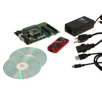
DV164136 Microchip Technology, DV164136 Datasheet - Page 301

DV164136
Manufacturer Part Number
DV164136
Description
DEVELOPMENT KIT FOR PIC18
Manufacturer
Microchip Technology
Series
PIC®r
Type
MCUr
Datasheets
1.DM183032.pdf
(38 pages)
2.DV164136.pdf
(448 pages)
3.DV164136.pdf
(6 pages)
4.DV164136.pdf
(446 pages)
5.DV164136.pdf
(4 pages)
6.DV164136.pdf
(18 pages)
Specifications of DV164136
Contents
Board, Cables, CDs, PICkit™ 3 Programmer, Power Supply
Processor To Be Evaluated
PIC18F8722, PIC18F87J11
Interface Type
RS-232, USB
Operating Supply Voltage
3.3 V, 5 V
Silicon Manufacturer
Microchip
Core Architecture
PIC
Core Sub-architecture
PIC18
Silicon Core Number
PIC18F
Silicon Family Name
PIC18F8xxx
Kit Contents
PIC18 Exp Brd PICkit 3 Cable CD PSU
Lead Free Status / RoHS Status
Lead free / RoHS Compliant
For Use With/related Products
PIC18F8722, PIC18F87J11
Lead Free Status / Rohs Status
Lead free / RoHS Compliant
Available stocks
Company
Part Number
Manufacturer
Quantity
Price
Company:
Part Number:
DV164136
Manufacturer:
MICROCHIP
Quantity:
12 000
- DM183032 PDF datasheet
- DV164136 PDF datasheet #2
- DV164136 PDF datasheet #3
- DV164136 PDF datasheet #4
- DV164136 PDF datasheet #5
- DV164136 PDF datasheet #6
- Current page: 301 of 448
- Download datasheet (8Mb)
21.7
The A/D Converter in the PIC18F87J11 family of
devices includes a self-calibration feature which com-
pensates for any offset generated within the module.
The calibration process is automated and is initiated by
setting the ADCAL bit (ADCON1<6>). The next time
the GO/DONE bit is set, the module will perform a
“dummy” conversion (that is, with reading none of the
input channels) and store the resulting value internally
to compensate for the offset. Thus, subsequent offsets
will be compensated. An example of a calibration
routine is shown in Example 21-1.
The calibration process assumes that the device is in a
relatively steady-state operating condition. If A/D
calibration is used, it should be performed after each
device Reset or if there are other major changes in
operating conditions.
21.8
The selection of the automatic acquisition time and A/D
conversion clock is determined in part by the clock
source and frequency while in a power-managed
mode.
EXAMPLE 21-1:
© 2009 Microchip Technology Inc.
CALIBRATION
A/D Converter Calibration
Operation in Power-Managed
Modes
BSF
BCF
BCF
BSF
BSF
BSF
BTFSC
BRA
BCF
WDTCON,ADSHR
ANCON0,PCFG0
WDTCON,ADSHR
ADCON0,ADON
ADCON1,ADCAL
ADCON0,GO
ADCON0,GO
CALIBRATION
ADCON1,ADCAL
SAMPLE A/D CALIBRATION ROUTINE
;Enable write/read to the shared SFR
;Make Channel 0 analog
;Disable write/read to the shared SFR
;Enable A/D module
;Enable Calibration
;Start a dummy A/D conversion
;
;Wait for the dummy conversion to finish
;
;Calibration done, turn off calibration enable
;Proceed with the actual A/D conversion
PIC18F87J11 FAMILY
If the A/D is expected to operate while the device is in
a power-managed mode, the ACQT2:ACQT0 and
ADCS2:ADCS0 bits in ADCON1 should be updated in
accordance with the power-managed mode clock that
will be used. After the power-managed mode is entered
(either of the power-managed Run modes), an A/D
acquisition or conversion may be started. Once an
acquisition or conversion is started, the device should
continue to be clocked by the same power-managed
mode clock source until the conversion has been com-
pleted. If desired, the device may be placed into the
corresponding power-managed Idle mode during the
conversion.
If the power-managed mode clock frequency is less
than 1 MHz, the A/D RC clock source should be
selected.
Operation in the Sleep mode requires the A/D RC clock
to be selected. If bits, ACQT2:ACQT0, are set to ‘000’
and a conversion is started, the conversion will be
delayed one instruction cycle to allow execution of the
SLEEP instruction and entry to Sleep mode. The IDLEN
and SCS bits in the OSCCON register must have
already been cleared prior to starting the conversion.
DS39778D-page 301
Related parts for DV164136
Image
Part Number
Description
Manufacturer
Datasheet
Request
R

Part Number:
Description:
Manufacturer:
Microchip Technology Inc.
Datasheet:

Part Number:
Description:
Manufacturer:
Microchip Technology Inc.
Datasheet:

Part Number:
Description:
Manufacturer:
Microchip Technology Inc.
Datasheet:

Part Number:
Description:
Manufacturer:
Microchip Technology Inc.
Datasheet:

Part Number:
Description:
Manufacturer:
Microchip Technology Inc.
Datasheet:

Part Number:
Description:
Manufacturer:
Microchip Technology Inc.
Datasheet:

Part Number:
Description:
Manufacturer:
Microchip Technology Inc.
Datasheet:

Part Number:
Description:
Manufacturer:
Microchip Technology Inc.
Datasheet:


