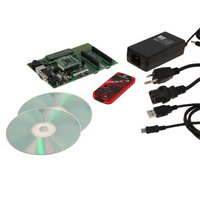
DV164136 Microchip Technology, DV164136 Datasheet - Page 142

DV164136
Manufacturer Part Number
DV164136
Description
DEVELOPMENT KIT FOR PIC18
Manufacturer
Microchip Technology
Series
PIC®r
Type
MCUr
Datasheets
1.DM183032.pdf
(38 pages)
2.DV164136.pdf
(448 pages)
3.DV164136.pdf
(6 pages)
4.DV164136.pdf
(446 pages)
5.DV164136.pdf
(4 pages)
6.DV164136.pdf
(18 pages)
Specifications of DV164136
Contents
Board, Cables, CDs, PICkit™ 3 Programmer, Power Supply
Processor To Be Evaluated
PIC18F8722, PIC18F87J11
Interface Type
RS-232, USB
Operating Supply Voltage
3.3 V, 5 V
Silicon Manufacturer
Microchip
Core Architecture
PIC
Core Sub-architecture
PIC18
Silicon Core Number
PIC18F
Silicon Family Name
PIC18F8xxx
Kit Contents
PIC18 Exp Brd PICkit 3 Cable CD PSU
Lead Free Status / RoHS Status
Lead free / RoHS Compliant
For Use With/related Products
PIC18F8722, PIC18F87J11
Lead Free Status / Rohs Status
Lead free / RoHS Compliant
Available stocks
Company
Part Number
Manufacturer
Quantity
Price
Company:
Part Number:
DV164136
Manufacturer:
MICROCHIP
Quantity:
12 000
- DM183032 PDF datasheet
- DV164136 PDF datasheet #2
- DV164136 PDF datasheet #3
- DV164136 PDF datasheet #4
- DV164136 PDF datasheet #5
- DV164136 PDF datasheet #6
- Current page: 142 of 448
- Download datasheet (8Mb)
PIC18F87J11 FAMILY
TABLE 10-12:
DS39778D-page 142
RE0/AD8/
PMRD/P2D
RE1/AD9/
PMWR/P2C
RE2/AD10/
PMBE/P2B
RE3/AD11/
PMA13/P3C/
REFO
RE4/AD12/
PMA12/P3B
Legend:
Note 1:
Pin Name
2:
3:
4:
5:
O = Output, I = Input, DIG = Digital Output, ST = Schmitt Buffer Input, TTL = TTL Buffer Input,
x = Don’t care (TRIS bit does not affect port direction or is overridden for this option).
Default assignments for P1B/P1C and P3B/P3C when ECCPMX Configuration bit is set (80-pin devices only).
External memory interface I/O takes priority over all other digital and PMP I/O.
Available on 80-pin devices only.
Alternate assignment for ECCP2/P2A when ECCP2MX Configuration bit is cleared (all devices in Microcontroller mode).
Default configuration for PMP (PMPMX Configuration bit = 1).
Function
PMWR
PMRD
PMBE
AD10
AD11
AD12
PMA13
PMA12
AD8
AD9
P3C
P3B
REFO
PORTE FUNCTIONS
RE0
P2D
RE1
P2C
RE2
RE3
RE4
P2B
(3)
(3)
(1)
(1)
(3)
(3)
(3)
(5)
(5)
(5)
Setting
TRIS
0
1
x
x
x
x
0
0
1
x
x
x
x
0
0
1
x
x
x
0
0
1
x
x
x
0
x
0
1
x
x
x
0
I/O
O
O
O
O
O
O
O
O
O
O
O
O
O
O
O
O
O
O
O
O
O
I
I
I
I
I
I
I
I
I
I
I
I
Type
DIG
DIG
TTL
DIG
TTL
DIG
DIG
DIG
TTL
DIG
TTL
DIG
DIG
DIG
TTL
DIG
DIG
DIG
DIG
TTL
DIG
DIG
DIG
DIG
DIG
TTL
DIG
DIG
I/O
ST
ST
ST
ST
ST
LATE<0> data output.
PORTE<0> data input.
External memory interface, address/data bit 8 output.
External memory interface, data bit 8 input.
Parallel Master Port read strobe pin.
Parallel Master Port read pin.
ECCP2 Enhanced PWM output, channel D; takes priority over port
and PMP data. May be configured for tri-state during Enhanced PWM
shutdown events.
LATE<1> data output.
PORTE<1> data input.
External memory interface, address/data bit 9 output.
External memory interface, data bit 9 input.
Parallel Master Port write strobe pin.
Parallel Master Port write pin.
ECCP2 Enhanced PWM output, channel C; takes priority over port
and PMP data. May be configured for tri-state during Enhanced PWM
shutdown events.
LATE<2> data output.
PORTE<2> data input.
External memory interface, address/data bit 10 output.
External memory interface, data bit 10 input.
Parallel Master Port byte enable.
ECCP2 Enhanced PWM output, channel B; takes priority over port and
PMP data. May be configured for tri-state during Enhanced PWM
shutdown events.
LATE<3> data output.
PORTE<3> data input.
External memory interface, address/data bit 11 output.
External memory interface, data bit 11 input.
Parallel Master Port address.
ECCP3 Enhanced PWM output, channel C; takes priority over port
and PMP data. May be configured for tri-state during Enhanced PWM
shutdown events.
Reference output clock.
LATE<4> data output.
PORTE<4> data input.
External memory interface, address/data bit 12 output.
External memory interface, data bit 12 input.
Parallel Master Port address.
ECCP3 Enhanced PWM output, channel B; takes priority over port and
PMP data. May be configured for tri-state during Enhanced PWM
shutdown events.
Description
© 2009 Microchip Technology Inc.
(2)
(2)
(2)
(2)
(2)
(2)
(2)
(2)
(2)
(2)
Related parts for DV164136
Image
Part Number
Description
Manufacturer
Datasheet
Request
R

Part Number:
Description:
Manufacturer:
Microchip Technology Inc.
Datasheet:

Part Number:
Description:
Manufacturer:
Microchip Technology Inc.
Datasheet:

Part Number:
Description:
Manufacturer:
Microchip Technology Inc.
Datasheet:

Part Number:
Description:
Manufacturer:
Microchip Technology Inc.
Datasheet:

Part Number:
Description:
Manufacturer:
Microchip Technology Inc.
Datasheet:

Part Number:
Description:
Manufacturer:
Microchip Technology Inc.
Datasheet:

Part Number:
Description:
Manufacturer:
Microchip Technology Inc.
Datasheet:

Part Number:
Description:
Manufacturer:
Microchip Technology Inc.
Datasheet:


