PCM18XK1 Microchip Technology, PCM18XK1 Datasheet - Page 91
PCM18XK1
Manufacturer Part Number
PCM18XK1
Description
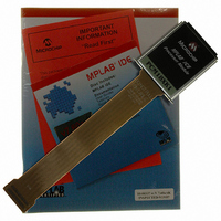
MODULE PROC PIC18F8680,6680,8565
Manufacturer
Microchip Technology
Datasheet
1.PCM18XK1.pdf
(496 pages)
Specifications of PCM18XK1
Accessory Type
Processor Module
Lead Free Status / RoHS Status
Not applicable / Not applicable
For Use With/related Products
ICE2000
For Use With
ICE2000 - EMULATOR MPLAB-ICE 2000 POD
Lead Free Status / Rohs Status
Lead free / RoHS Compliant


5.5
The minimum programming block is 4 words or 8 bytes.
Word or byte programming is not supported.
Table writes are used internally to load the holding
registers needed to program the Flash memory. There
are eight holding registers used by the table writes for
programming.
Since the Table Latch (TABLAT) is only a single byte,
the TBLWT instruction has to be executed 8 times for
each programming operation. All of the table write
operations will essentially be short writes because only
FIGURE 5-5:
2004 Microchip Technology Inc.
TBLPTR = xxxxx0
Writing to Flash Program Memory
Holding Register
8
TABLE WRITES TO FLASH PROGRAM MEMORY
TBLPTR = xxxxx1
Holding Register
PIC18F6585/8585/6680/8680
8
Program Memory
Write Register
TBLPTR = xxxxx2
TABLAT
the holding registers are written. At the end of updating
eight registers, the EECON1 register must be written
to, to start the programming operation with a long write.
The long write is necessary for programming the inter-
nal Flash. Instruction execution is halted while in a long
write cycle. The long write will be terminated by the
internal programming timer.
The EEPROM on-chip timer controls the write time.
The write/erase voltages are generated by an on-chip
charge pump, rated to operate over the voltage range
of the device for byte or word operations.
Holding Register
8
TBLPTR = xxxxx7
Holding Register
DS30491C-page 89
8
Related parts for PCM18XK1
Image
Part Number
Description
Manufacturer
Datasheet
Request
R

Part Number:
Description:
Manufacturer:
Microchip Technology Inc.
Datasheet:
Part Number:
Description:
Manufacturer:
Microchip Technology Inc.
Datasheet:
Part Number:
Description:
Manufacturer:
Microchip Technology Inc.
Datasheet:
Part Number:
Description:
Manufacturer:
Microchip Technology Inc.
Datasheet:
Part Number:
Description:
Manufacturer:
Microchip Technology Inc.
Datasheet:
Part Number:
Description:
Manufacturer:
Microchip Technology Inc.
Datasheet:
Part Number:
Description:
Manufacturer:
Microchip Technology Inc.
Datasheet:
Part Number:
Description:
Manufacturer:
Microchip Technology Inc.
Datasheet: