PCM18XK1 Microchip Technology, PCM18XK1 Datasheet - Page 486
PCM18XK1
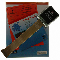
Manufacturer Part Number
PCM18XK1
Description
MODULE PROC PIC18F8680,6680,8565
Manufacturer
Microchip Technology
Datasheet
1.PCM18XK1.pdf
(496 pages)
Specifications of PCM18XK1
Accessory Type
Processor Module
Lead Free Status / RoHS Status
Not applicable / Not applicable
For Use With/related Products
ICE2000
For Use With
ICE2000 - EMULATOR MPLAB-ICE 2000 POD
Lead Free Status / Rohs Status
Lead free / RoHS Compliant


PIC18F6585/8585/6680/8680
Timer2 ............................................................................... 162
Timer3 ............................................................................... 164
Timing Diagrams
DS30491C-page 484
Associated Registers ................................................ 163
Operation .................................................................. 162
Postscaler. See Postscaler, Timer2.
PR2 Register............................................. 162, 173, 177
Prescaler. See Prescaler, Timer2.
SSP Clock Shift................................................. 162, 163
TMR2 Register .......................................................... 162
TMR2 to PR2 Match
Associated Registers ................................................ 166
Operation .................................................................. 165
Oscillator ........................................................... 164, 166
Overflow Interrupt ............................................. 164, 166
Special Event Trigger
TMR3H Register ....................................................... 164
TMR3L Register ........................................................ 164
A/D Conversion ......................................................... 447
Acknowledge Sequence ........................................... 222
Asynchronous Reception .......................................... 241
Asynchronous Transmission ..................................... 238
Asynchronous Transmission
Automatic Baud Rate
Auto-Wake-up Bit (WUE) During
Auto-Wake-up Bit (WUE)
Baud Rate Generator with
BRG Reset Due to SDA Arbitration During
Brown-out Reset (BOR) ............................................ 433
Bus Collision During a Repeated
Bus Collision During a Repeated
Bus Collision During a Stop Condition
Bus Collision During a Stop Condition
Bus Collision During Start Condition
Bus Collision During Start Condition
Bus Collision for Transmit and
Capture/Compare/PWM
CLKO and I/O ........................................................... 429
Clock Synchronization .............................................. 209
Clock/Instruction Cycle ............................................... 56
Example SPI Master Mode
Example SPI Master Mode
Interrupt..................................... 162, 163, 173, 177
(CCP) ................................................................ 166
(Back to Back)................................................... 238
Calculation ........................................................ 236
Normal Operation.............................................. 242
During Sleep ..................................................... 242
Clock Arbitration................................................ 216
Start Condition .................................................. 225
Start Condition (Case 1) ................................... 226
Start Condition (Case 2) ................................... 226
(Case 1) ............................................................ 227
(Case 2) ............................................................ 227
(SCL = 0) .......................................................... 225
(SDA only)......................................................... 224
(All CCP Modules) ............................................ 435
(CKE = 0) .......................................................... 437
(CKE = 1) .......................................................... 438
Acknowledge.................................................... 223
Example SPI Slave Mode
Example SPI Slave Mode
External Clock (All Modes
External Program Memory Bus
First Start Bit ............................................................. 217
Full-Bridge PWM Output........................................... 181
Half-Bridge PWM Output .......................................... 180
I
I
I
I
I
I
I
I
I
I
Low-Voltage Detect .................................................. 272
Master SSP I
Master SSP I
Parallel Slave Port
Parallel Slave Port (PSP)
Parallel Slave Port (PSP)
Program Memory Read ............................................ 430
Program Memory Write............................................. 431
PWM Auto-Shutdown (PRSEN = 0,
PWM Auto-Shutdown (PRSEN = 1,
PWM Output ............................................................. 173
Repeat Start Condition ............................................. 218
Reset, Watchdog Timer (WDT),
Send Break Character Sequence ............................. 243
Slave Mode General Call Address
Slave Synchronization .............................................. 195
Slow Rise Time (MCLR Tied to V
SPI Mode (Master Mode).......................................... 194
SPI Mode (Slave Mode with
2
2
2
2
2
2
2
2
2
2
C Bus Data............................................................. 441
C Bus Start/Stop Bits ............................................. 441
C Master Mode (7 or
C Master Mode
C Slave Mode (10-bit Reception,
C Slave Mode (10-bit Reception,
C Slave Mode
C Slave Mode (7-bit Reception,
C Slave Mode (7-bit Reception,
C Slave Mode
(CKE = 0).......................................................... 439
(CKE = 1).......................................................... 440
except PLL) ...................................................... 428
(16-bit Mode) ...................................................... 99
10-bit Transmission) ......................................... 220
(7-bit Reception) ............................................... 221
SEN = 0) ........................................................... 206
SEN = 1) ........................................................... 211
(10-bit Transmission)........................................ 207
SEN = 0) ........................................................... 204
SEN = 1) ........................................................... 210
(7-bit Transmission).......................................... 205
Start/Stop Bits................................................... 443
(PIC18FXX8X).................................................. 436
Read ................................................................. 154
Write ................................................................. 153
Auto-Restart Disabled) ..................................... 186
Auto-Restart Enabled) ...................................... 186
Oscillator Start-up Timer (OST)
and Power-up Timer (PWRT) ........................... 432
Sequence (7 or 10-bit
Address Mode) ................................................. 212
via 1 k Resistor) ............................................... 50
CKE = 0) ........................................................... 196
2
2
C Bus Data......................................... 443
C Bus
2004 Microchip Technology Inc.
DD
Related parts for PCM18XK1
Image
Part Number
Description
Manufacturer
Datasheet
Request
R

Part Number:
Description:
Manufacturer:
Microchip Technology Inc.
Datasheet:
Part Number:
Description:
Manufacturer:
Microchip Technology Inc.
Datasheet:
Part Number:
Description:
Manufacturer:
Microchip Technology Inc.
Datasheet:
Part Number:
Description:
Manufacturer:
Microchip Technology Inc.
Datasheet:
Part Number:
Description:
Manufacturer:
Microchip Technology Inc.
Datasheet:
Part Number:
Description:
Manufacturer:
Microchip Technology Inc.
Datasheet:
Part Number:
Description:
Manufacturer:
Microchip Technology Inc.
Datasheet:
Part Number:
Description:
Manufacturer:
Microchip Technology Inc.
Datasheet: