PCM18XK1 Microchip Technology, PCM18XK1 Datasheet - Page 256
PCM18XK1
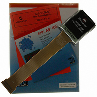
Manufacturer Part Number
PCM18XK1
Description
MODULE PROC PIC18F8680,6680,8565
Manufacturer
Microchip Technology
Datasheet
1.PCM18XK1.pdf
(496 pages)
Specifications of PCM18XK1
Accessory Type
Processor Module
Lead Free Status / RoHS Status
Not applicable / Not applicable
For Use With/related Products
ICE2000
For Use With
ICE2000 - EMULATOR MPLAB-ICE 2000 POD
Lead Free Status / Rohs Status
Lead free / RoHS Compliant


PIC18F6585/8585/6680/8680
19.1
For the A/D converter to meet its specified accuracy,
the charge holding capacitor (C
to fully charge to the input channel voltage level. The
analog input model is shown in Figure 19-2. The
source impedance (R
switch (R
required to charge the capacitor C
switch (R
(V
at the analog input (due to pin leakage current). The
maximum recommended impedance for analog
sources is 2.5 k . After the analog input channel is
selected (changed), this acquisition must be done
before the conversion can be started.
To
Equation 19-1 may be used. This equation assumes
that 1/2 LSb error is used (1024 steps for the A/D). The
1/2 LSb error is the maximum error allowed for the A/D
to meet its specified resolution.
Example 19-1 shows the calculation of the minimum
required acquisition time, T
on the following application system assumptions:
C
Rs
Conversion Error
V
Temperature
V
EQUATION 19-1:
EQUATION 19-2:
EXAMPLE 19-1:
DS30491C-page 254
T
V
or
T
T
Temperature coefficient is only required for temperatures > 25 C.
T
T
T
HOLD
DD
HOLD
ACQ
C
ACQ
ACQ
C
ACQ
DD
Note:
HOLD
). The source impedance affects the offset voltage
calculate
A/D Acquisition Requirements
SS
=
=
=
=
=
=
SS
=
=
) impedance varies over the device voltage
When the conversion is started, the
holding capacitor is disconnected from the
input pin.
) impedance directly affect the time
T
2 s + T
-C
-120 pF (1 k + 7 k + 2.5 k ) ln(0.0004885)
-120 pF (10.5 k ) ln(0.0004885)
-1.26 s (-7.6241)
9.61 s
2 s + 9.61 s + [(50 C – 25 C)(0.05 s/ C)]
11.61 s + 1.25 s
12.86 s
Amplifier Settling Time + Holding Capacitor Charging Time + Temperature Coefficient
T
(V
-(120 pF)(1 k + R
AMP
AMP
the
REF
HOLD
=
=
=
=
=
+ T
+ T
– (V
ACQUISITION TIME
A/D MINIMUM CHARGING TIME
CALCULATING THE MINIMUM REQUIRED ACQUISITION TIME
C
S
(R
minimum
C
) and the internal sampling
C
+ [(Temp – 25 C)(0.05 s/ C)]
120 pF
2.5 k
1/2 LSb
5V
50 C (system max.)
0V @ time = 0
IC
REF
ACQ
+ T
+ T
+ R
/2048)) • (1 – e
COFF
COFF
. This calculation is based
Rss = 7 k
SS
HOLD
SS
+ R
HOLD
acquisition
+ R
) must be allowed
S
) ln(1/2047)
S
. The sampling
) ln(1/2047)
(-Tc/C
HOLD
time,
(R
IC
+ R
SS
+ R
S
))
19.2
If external voltage references are used instead of the
internal AV
of the V
ered. During acquisition, currents supplied by these
sources are insignificant. However, during conversion,
the A/D module sinks and sources current through the
reference sources. The effect of this current, as specified
in parameter A50, along with source impedance must be
considered to meet specified A/D resolution.
)
Note:
REF
A/D V
DD
+ and V
To maintain the best possible performance
in A/D conversions, external V
should be buffered with an operational
amplifier or other low output impedance
circuit.
When using external voltage references
with the A/D converter, the source imped-
ance of the external voltage references
must be less than 20 to obtain the spec-
ified A/D resolution. Higher reference
source impedances will increase both
offset and gain errors. Resistive voltage
dividers will not provide a sufficiently low
source impedance.
and AV
REF
REF
+ and V
SS
- voltage sources must be consid-
sources, the source impedance
2004 Microchip Technology Inc.
REF
- References
REF
inputs
Related parts for PCM18XK1
Image
Part Number
Description
Manufacturer
Datasheet
Request
R

Part Number:
Description:
Manufacturer:
Microchip Technology Inc.
Datasheet:
Part Number:
Description:
Manufacturer:
Microchip Technology Inc.
Datasheet:
Part Number:
Description:
Manufacturer:
Microchip Technology Inc.
Datasheet:
Part Number:
Description:
Manufacturer:
Microchip Technology Inc.
Datasheet:
Part Number:
Description:
Manufacturer:
Microchip Technology Inc.
Datasheet:
Part Number:
Description:
Manufacturer:
Microchip Technology Inc.
Datasheet:
Part Number:
Description:
Manufacturer:
Microchip Technology Inc.
Datasheet:
Part Number:
Description:
Manufacturer:
Microchip Technology Inc.
Datasheet: