PCM18XK1 Microchip Technology, PCM18XK1 Datasheet - Page 481
PCM18XK1
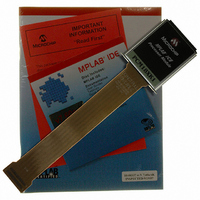
Manufacturer Part Number
PCM18XK1
Description
MODULE PROC PIC18F8680,6680,8565
Manufacturer
Microchip Technology
Datasheet
1.PCM18XK1.pdf
(496 pages)
Specifications of PCM18XK1
Accessory Type
Processor Module
Lead Free Status / RoHS Status
Not applicable / Not applicable
For Use With/related Products
ICE2000
For Use With
ICE2000 - EMULATOR MPLAB-ICE 2000 POD
Lead Free Status / Rohs Status
Lead free / RoHS Compliant


MSSP Module
MULLW ............................................................................. 392
MULWF ............................................................................. 392
N
NEGF ................................................................................ 393
NOP .................................................................................. 393
Normal Operation Mode.................................................... 328
O
Opcode Field Descriptions ................................................ 366
OPTION_REG Register
Oscillator Configuration....................................................... 23
2004 Microchip Technology Inc.
I
Overview ................................................................... 189
SPI Mode .................................................................. 189
SPI Mode. See SPI.
SSPBUF Register ..................................................... 194
SSPSR Register ....................................................... 194
SPI Master/Slave Connection ................................... 193
PSA Bit...................................................................... 157
T0CS Bit.................................................................... 157
T0PS2:T0PS0 Bits .................................................... 157
T0SE Bit.................................................................... 157
EC ............................................................................... 23
ECIO ........................................................................... 23
ECIO+PLL................................................................... 23
ECIO+SPLL ................................................................ 23
HS ............................................................................... 23
HS+PLL ...................................................................... 23
HS+SPLL .................................................................... 23
LP................................................................................ 23
RC............................................................................... 23
RCIO ........................................................................... 23
XT ............................................................................... 23
2
C Mode. See I
Master Mode ..................................................... 213
Master Mode Start Condition ............................ 217
Module Operation ............................................. 202
Multi-Master Communication,
Multi-Master Mode ............................................ 223
Registers........................................................... 198
Slave Mode ....................................................... 202
Slave Mode, Addressing ................................... 202
Slave Mode, Reception..................................... 203
Slave Mode, Transmission ............................... 203
Sleep Operation ................................................ 223
Stop Condition Timing ...................................... 222
Associated Registers ........................................ 197
Bus Mode Compatibility .................................... 197
Effects of a Reset ............................................. 197
Enabling SPI I/O ............................................... 193
Master Mode ..................................................... 194
Operation .......................................................... 192
Slave Mode ....................................................... 195
Slave Select
Sleep Operation ................................................ 197
SPI Clock .......................................................... 194
Typical Connection ........................................... 193
Reception.................................................. 219
Repeated Start Condition
Transmission ............................................ 219
Bus Collision and
Arbitration ................................................. 223
Synchronization ........................................ 195
Timing ............................................... 218
2
C.
PIC18F6585/8585/6680/8680
Oscillator Selection ........................................................... 345
Oscillator Start-up Timer (OST) .................................. 34, 345
Oscillator Switching Feature
Oscillator, Timer1.............................................. 159, 161, 166
Oscillator, Timer3.............................................................. 164
Oscillator, WDT................................................................. 355
P
Packaging ......................................................................... 465
Parallel Slave Port (PSP).......................................... 133, 152
Parallel Slave Port Requirements
Phase Locked Loop (PLL) .................................................. 25
PICkit 1 Flash Starter Kit .................................................. 411
PICSTART Plus Development
PIE Registers.................................................................... 117
Pin Functions
System Clock Switch Bit............................................. 27
Details....................................................................... 466
Marking..................................................................... 465
Associated Registers................................................ 154
RE0/RD/AD8 Pin ...................................................... 152
RE1/WR/AD9 Pin ..................................................... 152
RE2/CS/AD10 Pin .................................................... 152
Select (PSPMODE Bit) ..................................... 133, 152
(PIC18FXX8X).......................................................... 436
Programmer.............................................................. 410
AV
AV
OSC1/CLKI ................................................................. 12
OSC2/CLKO/RA6 ....................................................... 12
RA0/AN0..................................................................... 13
RA1/AN1..................................................................... 13
RA2/AN2/V
RA3/AN3/V
RA4/T0CKI ................................................................. 13
RA5/AN4/LVDIN ......................................................... 13
RA6............................................................................. 13
RB0/INT0.................................................................... 14
RB1/INT1.................................................................... 14
RB2/INT2.................................................................... 14
RB3/INT3/CCP2 ......................................................... 14
RB4/KBI0.................................................................... 14
RB5/KBI1/PGM........................................................... 14
RB6/KBI2/PGC ........................................................... 14
RB7/KBI3/PGD ........................................................... 14
RC0/T1OSO/T13CKI .................................................. 15
RC1/T1OSI/CCP2 ...................................................... 15
RC2/CCP1/P1A .......................................................... 15
RC3/SCK/SCL ............................................................ 15
RC4/SDI/SDA ............................................................. 15
RC5/SDO.................................................................... 15
RC6/TX/CK ................................................................. 15
RC7/RX/DT................................................................. 15
RD0/PSP0/AD0 .......................................................... 16
RD1/PSP1/AD1 .......................................................... 16
RD2/PSP2/AD2 .......................................................... 16
RD3/PSP3/AD3 .......................................................... 16
RD4/PSP4/AD4 .......................................................... 16
RD5/PSP5/AD5 .......................................................... 16
RD6/PSP6/AD6 .......................................................... 16
RD7/PSP7/AD7 .......................................................... 16
RE0/RD/AD8 .............................................................. 17
RE1/WR/AD9.............................................................. 17
DD
SS
........................................................................... 21
........................................................................... 21
REF
REF
- .......................................................... 13
+ ......................................................... 13
DS30491C-page 479
Related parts for PCM18XK1
Image
Part Number
Description
Manufacturer
Datasheet
Request
R

Part Number:
Description:
Manufacturer:
Microchip Technology Inc.
Datasheet:
Part Number:
Description:
Manufacturer:
Microchip Technology Inc.
Datasheet:
Part Number:
Description:
Manufacturer:
Microchip Technology Inc.
Datasheet:
Part Number:
Description:
Manufacturer:
Microchip Technology Inc.
Datasheet:
Part Number:
Description:
Manufacturer:
Microchip Technology Inc.
Datasheet:
Part Number:
Description:
Manufacturer:
Microchip Technology Inc.
Datasheet:
Part Number:
Description:
Manufacturer:
Microchip Technology Inc.
Datasheet:
Part Number:
Description:
Manufacturer:
Microchip Technology Inc.
Datasheet: