PCM18XK1 Microchip Technology, PCM18XK1 Datasheet - Page 250
PCM18XK1
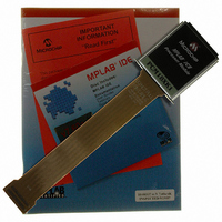
Manufacturer Part Number
PCM18XK1
Description
MODULE PROC PIC18F8680,6680,8565
Manufacturer
Microchip Technology
Datasheet
1.PCM18XK1.pdf
(496 pages)
Specifications of PCM18XK1
Accessory Type
Processor Module
Lead Free Status / RoHS Status
Not applicable / Not applicable
For Use With/related Products
ICE2000
For Use With
ICE2000 - EMULATOR MPLAB-ICE 2000 POD
Lead Free Status / Rohs Status
Lead free / RoHS Compliant


PIC18F6585/8585/6680/8680
18.4.2
The operation of the Synchronous Master and Slave
modes is identical, except in the case of Sleep or any
Idle mode and bit SREN, which is a “don’t care” in
Slave mode.
If receive is enabled by setting the CREN bit prior to
entering Sleep or any Idle mode, then a word may be
received while in this low-power mode. Once the word
is received, the RSR register will transfer the data to the
RCREG register; if the RCIE enable bit is set, the inter-
rupt generated will wake the chip from low-power
mode. If the global interrupt is enabled, the program will
branch to the interrupt vector.
TABLE 18-10: REGISTERS ASSOCIATED WITH SYNCHRONOUS SLAVE RECEPTION
DS30491C-page 248
INTCON
PIR1
PIE1
IPR1
RCSTA
RCREG
TXSTA
BAUDCON
SPBRGH
SPBRG
Legend:
Name
x = unknown, - = unimplemented, read as ‘0’. Shaded cells are not used for synchronous slave reception.
USART Receive Register
Baud Rate Generator Register, High Byte
Baud Rate Generator Register, Low Byte
USART SYNCHRONOUS SLAVE
RECEPTION
GIE/GIEH
PSPIF
PSPIE
PSPIP
CSRC
SPEN
Bit 7
—
PEIE/GIEL
RCIDL
ADIF
ADIE
ADIP
Bit 6
RX9
TX9
TMR0IE
SREN
TXEN
RCIF
RCIE
RCIP
Bit 5
—
INT0IE
CREN
SYNC
SCKP
TXIE
TXIP
Bit 4
TXIF
ADDEN
SENDB
BRG16
SSPIE
SSPIP
SSPIF
RBIE
Bit 3
To set up a synchronous slave reception:
1.
2.
3.
4.
5.
6.
7.
8.
9.
TMR0IF
CCP1IF
CCP1IE
CCP1IP
BRGH
FERR
Bit 2
—
Enable the synchronous master serial port by
setting bits SYNC and SPEN and clearing bit
CSRC.
If interrupts are desired, set enable bit RCIE.
If 9-bit reception is desired, set bit RX9.
To enable reception, set enable bit CREN.
Flag bit RCIF will be set when reception is
complete. An interrupt will be generated if
enable bit RCIE was set.
Read the RCSTA register to get the 9th bit (if
enabled) and determine if any error occurred
during reception.
Read the 8-bit received data by reading the
RCREG register.
If any error occurred, clear the error by clearing
bit CREN.
If using interrupts, ensure that the GIE and PEIE
bits in the INTCON register (INTCON<7:6>) are
set.
TMR2IF
TMR2IE
TMR2IP
INT0IF
OERR
TRMT
WUE
Bit 1
TMR1IF
TMR1IE
TMR1IP
ABDEN
RX9D
TX9D
RBIF
Bit 0
2004 Microchip Technology Inc.
0000 0000
0000 0000
0000 0000
1111 1111
0000 000x
0000 0000
0000 0010
-1-0 0-00
0000 0000
0000 0000
POR, BOR
Value on
0000 0000
0000 0000
0000 0000
1111 1111
0000 000x
0000 0000
0000 0010
-1-0 0-00
0000 0000
0000 0000
Value on
all other
Resets
Related parts for PCM18XK1
Image
Part Number
Description
Manufacturer
Datasheet
Request
R

Part Number:
Description:
Manufacturer:
Microchip Technology Inc.
Datasheet:
Part Number:
Description:
Manufacturer:
Microchip Technology Inc.
Datasheet:
Part Number:
Description:
Manufacturer:
Microchip Technology Inc.
Datasheet:
Part Number:
Description:
Manufacturer:
Microchip Technology Inc.
Datasheet:
Part Number:
Description:
Manufacturer:
Microchip Technology Inc.
Datasheet:
Part Number:
Description:
Manufacturer:
Microchip Technology Inc.
Datasheet:
Part Number:
Description:
Manufacturer:
Microchip Technology Inc.
Datasheet:
Part Number:
Description:
Manufacturer:
Microchip Technology Inc.
Datasheet: