PCM18XK1 Microchip Technology, PCM18XK1 Datasheet - Page 166
PCM18XK1
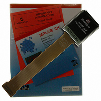
Manufacturer Part Number
PCM18XK1
Description
MODULE PROC PIC18F8680,6680,8565
Manufacturer
Microchip Technology
Datasheet
1.PCM18XK1.pdf
(496 pages)
Specifications of PCM18XK1
Accessory Type
Processor Module
Lead Free Status / RoHS Status
Not applicable / Not applicable
For Use With/related Products
ICE2000
For Use With
ICE2000 - EMULATOR MPLAB-ICE 2000 POD
Lead Free Status / Rohs Status
Lead free / RoHS Compliant


PIC18F6585/8585/6680/8680
14.0
The Timer3 module timer/counter has the following
features:
• 16-bit timer/counter
• Readable and writable (both registers)
• Internal or external clock select
• Interrupt on overflow from FFFFh to 0000h
• Reset from CCP module trigger
REGISTER 14-1:
DS30491C-page 164
(two 8-bit registers; TMR3H and TMR3L)
TIMER3 MODULE
bit 7
bit 6, 3 T3CCP2:T3CCP1: Timer3 and Timer1 to CCPx Enable bits
bit 5-4
bit 2
bit 1
bit 0
T3CON: TIMER3 CONTROL REGISTER
RD16: 16-bit Read/Write Mode Enable bit
1 = Enables register read/write of Timer3 in one 16-bit operation
0 = Enables register read/write of Timer3 in two 8-bit operations
1x = Timer3 is the clock source for compare/capture of CCP1 and CCP2 modules
01 = Timer3 is the clock source for compare/capture of CCP2 module,
00 = Timer1 is the clock source for compare/capture of CCP1 and CCP2 modules
T3CKPS1:T3CKPS0: Timer3 Input Clock Prescale Select bits
11 = 1:8 prescale value
10 = 1:4 prescale value
01 = 1:2 prescale value
00 = 1:1 prescale value
T3SYNC: Timer3 External Clock Input Synchronization Control bit
(Not usable if the system clock comes from Timer1/Timer3.)
When TMR3CS = 1:
1 = Do not synchronize external clock input
0 = Synchronize external clock input
When TMR3CS = 0:
This bit is ignored. Timer3 uses the internal clock when TMR3CS = 0.
TMR3CS: Timer3 Clock Source Select bit
1 = External clock input from Timer1 oscillator or T13CKI
0 = Internal clock (F
TMR3ON: Timer3 On bit
1 = Enables Timer3
0 = Stops Timer3
bit 7
Legend:
R = Readable bit
- n = Value at POR
R/W-0
RD16
(on the rising edge after the first falling edge)
Timer1 is the clock source for compare/capture of CCP1 module
T3CCP2
R/W-0
OSC
T3CKPS1
/4)
R/W-0
W = Writable bit
‘1’ = Bit is set
T3CKPS0
R/W-0
Figure 14-1 is a simplified block diagram of the Timer3
module.
Register 14-1 shows the Timer3 Control register. This
register controls the operating mode of the Timer3
module and sets the Enhanced CCP1 and CCP2 clock
source.
Register 12-1 shows the Timer1 Control register. This
register controls the operating mode of the Timer1
module, as well as containing the Timer1 oscillator
enable bit (T1OSCEN) which can be a clock source for
Timer3.
T3CCP1
R/W-0
U = Unimplemented bit, read as ‘0’
‘0’ = Bit is cleared
T3SYNC
R/W-0
2004 Microchip Technology Inc.
TMR3CS
x = Bit is unknown
R/W-0
TMR3ON
R/W-0
bit 0
Related parts for PCM18XK1
Image
Part Number
Description
Manufacturer
Datasheet
Request
R

Part Number:
Description:
Manufacturer:
Microchip Technology Inc.
Datasheet:
Part Number:
Description:
Manufacturer:
Microchip Technology Inc.
Datasheet:
Part Number:
Description:
Manufacturer:
Microchip Technology Inc.
Datasheet:
Part Number:
Description:
Manufacturer:
Microchip Technology Inc.
Datasheet:
Part Number:
Description:
Manufacturer:
Microchip Technology Inc.
Datasheet:
Part Number:
Description:
Manufacturer:
Microchip Technology Inc.
Datasheet:
Part Number:
Description:
Manufacturer:
Microchip Technology Inc.
Datasheet:
Part Number:
Description:
Manufacturer:
Microchip Technology Inc.
Datasheet: