PCM18XK1 Microchip Technology, PCM18XK1 Datasheet - Page 161
PCM18XK1
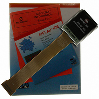
Manufacturer Part Number
PCM18XK1
Description
MODULE PROC PIC18F8680,6680,8565
Manufacturer
Microchip Technology
Datasheet
1.PCM18XK1.pdf
(496 pages)
Specifications of PCM18XK1
Accessory Type
Processor Module
Lead Free Status / RoHS Status
Not applicable / Not applicable
For Use With/related Products
ICE2000
For Use With
ICE2000 - EMULATOR MPLAB-ICE 2000 POD
Lead Free Status / Rohs Status
Lead free / RoHS Compliant


12.0
The Timer1 module timer/counter has the following
features:
• 16-bit timer/counter
• Readable and writable (both registers)
• Internal or external clock select
• Interrupt on overflow from 0FFFFh to 0000h
• Reset from CCP module special event trigger
REGISTER 12-1:
2004 Microchip Technology Inc.
(two 8-bit registers; TMR1H and TMR1L)
TIMER1 MODULE
bit 7
bit 6
bit 5-4
bit 3
bit 2
bit 1
bit 0
RD16: 16-bit Read/Write Mode Enable bit
1 = Enables register read/write of Timer1 in one 16-bit operation
0 = Enables register read/write of Timer1 in two 8-bit operations
Unimplemented: Read as ‘0’
T1CKPS1:T1CKPS0: Timer1 Input Clock Prescale Select bits
11 = 1:8 prescale value
10 = 1:4 prescale value
01 = 1:2 prescale value
00 = 1:1 prescale value
T1OSCEN: Timer1 Oscillator Enable bit
1 = Timer1 oscillator is enabled
0 = Timer1 oscillator is shut-off
The oscillator inverter and feedback resistor are turned off to eliminate power drain.
T1SYNC: Timer1 External Clock Input Synchronization Select bit
When TMR1CS = 1:
1 = Do not synchronize external clock input
0 = Synchronize external clock input
When TMR1CS = 0:
This bit is ignored. Timer1 uses the internal clock when TMR1CS = 0.
TMR1CS: Timer1 Clock Source Select bit
1 = External clock from pin RC0/T1OSO/T13CKI (on the rising edge)
0 = Internal clock (F
TMR1ON: Timer1 On bit
1 = Enables Timer1
0 = Stops Timer1
bit 7
Legend:
R = Readable bit
- n = Value at POR
T1CON: TIMER1 CONTROL REGISTER
R/W-0
RD16
U-0
—
OSC
T1CKPS1
/4)
PIC18F6585/8585/6680/8680
R/W-0
W = Writable bit
‘1’ = Bit is set
T1CKPS0
R/W-0
Figure 12-1 is a simplified block diagram of the Timer1
module.
Register 12-1 details the Timer1 Control register. This
register controls the operating mode of the Timer1
module and contains the Timer1 Oscillator Enable bit
(T1OSCEN). Timer1 can be enabled or disabled by
setting or clearing control bit, TMR1ON (T1CON<0>).
T1OSCEN
R/W-0
U = Unimplemented bit, read as ‘0’
‘0’ = Bit is cleared
T1SYNC
R/W-0
TMR1CS
x = Bit is unknown
R/W-0
DS30491C-page 159
TMR1ON
R/W-0
bit 0
Related parts for PCM18XK1
Image
Part Number
Description
Manufacturer
Datasheet
Request
R

Part Number:
Description:
Manufacturer:
Microchip Technology Inc.
Datasheet:
Part Number:
Description:
Manufacturer:
Microchip Technology Inc.
Datasheet:
Part Number:
Description:
Manufacturer:
Microchip Technology Inc.
Datasheet:
Part Number:
Description:
Manufacturer:
Microchip Technology Inc.
Datasheet:
Part Number:
Description:
Manufacturer:
Microchip Technology Inc.
Datasheet:
Part Number:
Description:
Manufacturer:
Microchip Technology Inc.
Datasheet:
Part Number:
Description:
Manufacturer:
Microchip Technology Inc.
Datasheet:
Part Number:
Description:
Manufacturer:
Microchip Technology Inc.
Datasheet: