PCM18XK1 Microchip Technology, PCM18XK1 Datasheet - Page 178
PCM18XK1
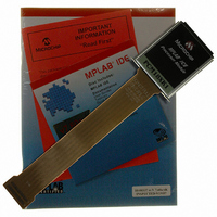
Manufacturer Part Number
PCM18XK1
Description
MODULE PROC PIC18F8680,6680,8565
Manufacturer
Microchip Technology
Datasheet
1.PCM18XK1.pdf
(496 pages)
Specifications of PCM18XK1
Accessory Type
Processor Module
Lead Free Status / RoHS Status
Not applicable / Not applicable
For Use With/related Products
ICE2000
For Use With
ICE2000 - EMULATOR MPLAB-ICE 2000 POD
Lead Free Status / Rohs Status
Lead free / RoHS Compliant


PIC18F6585/8585/6680/8680
16.1
The enhanced CCP module may have up to four
outputs depending on the selected operating mode.
These outputs, designated P1A through P1D, are
multiplexed with I/O pins RC2, RE6, RE5 and RG4.
The pin assignments are summarized in Table 16-1.
TABLE 16-1:
FIGURE 16-1:
DS30491C-page 176
Compatible CCP
Dual PWM
Quad PWM
Legend: x = Don’t care. Shaded cells indicate pin assignments not used by ECCP in a given mode.
Note 1:
ECCP Mode
RB3/CCP1/P1A pin
Special Event Trigger will:
2:
Reset Timer1 or Timer3, but will not set Timer1 or Timer3 interrupt flag bit
and set bit GO/DONE (ADCON0<2>) which starts an A/D conversion.
ECCP Outputs
TRIS register values must be configured appropriately.
On PIC18F8X8X devices, these pins can be alternately multiplexed with RH7 or RH6 by changing the
ECCPMX configuration bit.
Output Enable
PIN ASSIGNMENTS FOR VARIOUS ECCP MODES
Configuration
TRISB<3>
CCP1CON
00xx11xx
10xx11xx
x1xx11xx
COMPARE MODE OPERATION BLOCK DIAGRAM
Q
R
S
CCP1
RC2
P1A
P1A
CCP1CON<3:0>
Mode Select
Output
Logic
P1B
P1B
RE6
RE6
Set Flag bit CCP1IF
(2)
(2)
Match
To configure I/O pins as PWM outputs, the proper PWM
mode must be selected by setting the P1Mx and
CCP1Mx bits (CCP1CON<7:6> and <3:0>, respec-
tively). The appropriate TRIS direction bits for the port
pins must also be set as outputs.
P1C
RE5
RE5
RE5
TMR1H
(2)
T3CCP2
TMR1L
CCPR1H CCPR1L
2004 Microchip Technology Inc.
Comparator
0
1
TMR3H
RG4
RG4
RG4
P1D
TMR3L
Related parts for PCM18XK1
Image
Part Number
Description
Manufacturer
Datasheet
Request
R

Part Number:
Description:
Manufacturer:
Microchip Technology Inc.
Datasheet:
Part Number:
Description:
Manufacturer:
Microchip Technology Inc.
Datasheet:
Part Number:
Description:
Manufacturer:
Microchip Technology Inc.
Datasheet:
Part Number:
Description:
Manufacturer:
Microchip Technology Inc.
Datasheet:
Part Number:
Description:
Manufacturer:
Microchip Technology Inc.
Datasheet:
Part Number:
Description:
Manufacturer:
Microchip Technology Inc.
Datasheet:
Part Number:
Description:
Manufacturer:
Microchip Technology Inc.
Datasheet:
Part Number:
Description:
Manufacturer:
Microchip Technology Inc.
Datasheet: