PCM18XK1 Microchip Technology, PCM18XK1 Datasheet - Page 263
PCM18XK1
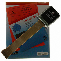
Manufacturer Part Number
PCM18XK1
Description
MODULE PROC PIC18F8680,6680,8565
Manufacturer
Microchip Technology
Datasheet
1.PCM18XK1.pdf
(496 pages)
Specifications of PCM18XK1
Accessory Type
Processor Module
Lead Free Status / RoHS Status
Not applicable / Not applicable
For Use With/related Products
ICE2000
For Use With
ICE2000 - EMULATOR MPLAB-ICE 2000 POD
Lead Free Status / Rohs Status
Lead free / RoHS Compliant


20.2
A single comparator is shown in Figure 20-2, along with
the relationship between the analog input levels and
the digital output. When the analog input at V
than the analog input V
is a digital low level. When the analog input at V
greater than the analog input V
comparator is a digital high level. The shaded areas of
the output of the comparator in Figure 20-2 represent
the uncertainty due to input offsets and response time.
20.3
An external or internal reference signal may be used
depending on the Comparator Operating mode. The
analog signal present at V
at V
adjusted accordingly (Figure 20-2).
FIGURE 20-2:
20.3.1
When external voltage references are used, the
comparator module can be configured to have the com-
parators operate from the same or different reference
sources. However, threshold detector applications may
require the same reference. The reference signal must
be between V
pin of the comparator(s).
2004 Microchip Technology Inc.
Output
V
V
Output
IN
IN
V
V
IN
IN–
IN+
-
+
+ and the digital output of the comparator is
V
V
IN
IN
Comparator Operation
Comparator Reference
+
-
EXTERNAL REFERENCE SIGNAL
SS
and V
+
–
SINGLE COMPARATOR
IN
DD
-, the output of the comparator
IN
and can be applied to either
- is compared to the signal
IN
-, the output of the
Output
IN
PIC18F6585/8585/6680/8680
+ is less
IN
+ is
20.3.2
The comparator module also allows the selection of an
internally generated voltage reference for the compara-
tors. Section 21.0 “Comparator Voltage Reference
Module” contains a detailed description of the compar-
ator voltage reference module that provides this signal.
The internal reference signal is used when comparators
are in mode CM<2:0> = 110 (Figure 20-1). In this mode,
the internal voltage reference is applied to the V
of both comparators.
20.4
Response time is the minimum time, after selecting a
new reference voltage or input source, before the
comparator output has a valid level. If the internal
reference is changed, the maximum delay of the inter-
nal voltage reference must be considered when using
the comparator outputs. Otherwise, the maximum
delay of the comparators should be used (Section 27.0
“Electrical Characteristics”).
20.5
The comparator outputs are read through the CMCON
register. These bits are read-only. The comparator
outputs may also be directly output to the RF1 and RF2
I/O pins. When enabled, multiplexors in the output path
of the RF1 and RF2 pins will switch and the output of
each pin will be the unsynchronized output of the com-
parator. The uncertainty of each of the comparators is
related to the input offset voltage and the response time
given in the specifications. Figure 20-3 shows the
comparator output block diagram.
The TRISA bits will still function as an output
enable/disable for the RF1 and RF2 pins while in this
mode.
The polarity of the comparator outputs can be changed
using the C2INV and C1INV bits (CMCON<4:5>).
Note 1: When reading the Port register, all pins
2: Analog levels on any pin defined as a dig-
Comparator Response Time
Comparator Outputs
INTERNAL REFERENCE SIGNAL
configured as analog inputs will read as a
‘0’. Pins configured as digital inputs will
convert an analog input according to the
Schmitt Trigger input specification.
ital input may cause the input buffer to
consume more current than is specified.
DS30491C-page 261
IN
+ pin
Related parts for PCM18XK1
Image
Part Number
Description
Manufacturer
Datasheet
Request
R

Part Number:
Description:
Manufacturer:
Microchip Technology Inc.
Datasheet:
Part Number:
Description:
Manufacturer:
Microchip Technology Inc.
Datasheet:
Part Number:
Description:
Manufacturer:
Microchip Technology Inc.
Datasheet:
Part Number:
Description:
Manufacturer:
Microchip Technology Inc.
Datasheet:
Part Number:
Description:
Manufacturer:
Microchip Technology Inc.
Datasheet:
Part Number:
Description:
Manufacturer:
Microchip Technology Inc.
Datasheet:
Part Number:
Description:
Manufacturer:
Microchip Technology Inc.
Datasheet:
Part Number:
Description:
Manufacturer:
Microchip Technology Inc.
Datasheet: