PCM18XK1 Microchip Technology, PCM18XK1 Datasheet - Page 273
PCM18XK1
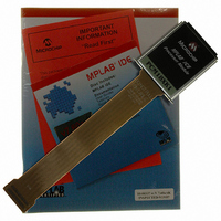
Manufacturer Part Number
PCM18XK1
Description
MODULE PROC PIC18F8680,6680,8565
Manufacturer
Microchip Technology
Datasheet
1.PCM18XK1.pdf
(496 pages)
Specifications of PCM18XK1
Accessory Type
Processor Module
Lead Free Status / RoHS Status
Not applicable / Not applicable
For Use With/related Products
ICE2000
For Use With
ICE2000 - EMULATOR MPLAB-ICE 2000 POD
Lead Free Status / Rohs Status
Lead free / RoHS Compliant


22.1
The Low-Voltage Detect Control register controls the
operation of the Low-Voltage Detect circuitry.
REGISTER 22-1:
2004 Microchip Technology Inc.
Control Register
bit 7-6
bit 5
bit 4
bit 3-0
LVDCON REGISTER
bit 7
Unimplemented: Read as ‘0’
IRVST: Internal Reference Voltage Stable Flag bit
1 = Indicates that the Low-Voltage Detect logic will generate the interrupt flag at the specified
0 = Indicates that the Low-Voltage Detect logic will not generate the interrupt flag at the
LVDEN: Low-Voltage Detect Power Enable bit
1 = Enables LVD, powers up LVD circuit
0 = Disables LVD, powers down LVD circuit
LVDL3:LVDL0: Low-Voltage Detection Limit bits
1111 = External analog input is used (input comes from the LVDIN pin)
1110 = 4.5V-4.77V
1101 = 4.2V-4.45V
1100 = 4.0V-4.24V
1011 = 3.8V-4.03V
1010 = 3.6V-3.82V
1001 = 3.5V-3.71V
1000 = 3.3V-3.50V
0111 = 3.0V-3.18V
0110 = 2.8V-2.97V
0101 = 2.7V-2.86V
0100 = 2.5V-2.65V
0011 = 2.4V-2.54V
0010 = 2.2V-2.33V
0001 = 2.0V-2.12V
0000 = Reserved
Legend:
R = Readable bit
- n = Value at POR
Note:
U-0
—
voltage range
specified voltage range and the LVD interrupt should not be enabled
LVDL3:LVDL0 modes which result in a trip point below the valid operating voltage
of the device are not tested.
U-0
—
PIC18F6585/8585/6680/8680
IRVST
R-0
W = Writable bit
‘1’ = Bit is set
LVDEN
R/W-0
U = Unimplemented bit, read as ‘0’
‘0’ = Bit is cleared
LVDL3
R/W-0
LVDL2
R/W-1
x = Bit is unknown
LVDL1
R/W-0
DS30491C-page 271
LVDL0
R/W-1
bit 0
Related parts for PCM18XK1
Image
Part Number
Description
Manufacturer
Datasheet
Request
R

Part Number:
Description:
Manufacturer:
Microchip Technology Inc.
Datasheet:
Part Number:
Description:
Manufacturer:
Microchip Technology Inc.
Datasheet:
Part Number:
Description:
Manufacturer:
Microchip Technology Inc.
Datasheet:
Part Number:
Description:
Manufacturer:
Microchip Technology Inc.
Datasheet:
Part Number:
Description:
Manufacturer:
Microchip Technology Inc.
Datasheet:
Part Number:
Description:
Manufacturer:
Microchip Technology Inc.
Datasheet:
Part Number:
Description:
Manufacturer:
Microchip Technology Inc.
Datasheet:
Part Number:
Description:
Manufacturer:
Microchip Technology Inc.
Datasheet: