PCM18XK1 Microchip Technology, PCM18XK1 Datasheet - Page 251
PCM18XK1
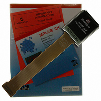
Manufacturer Part Number
PCM18XK1
Description
MODULE PROC PIC18F8680,6680,8565
Manufacturer
Microchip Technology
Datasheet
1.PCM18XK1.pdf
(496 pages)
Specifications of PCM18XK1
Accessory Type
Processor Module
Lead Free Status / RoHS Status
Not applicable / Not applicable
For Use With/related Products
ICE2000
For Use With
ICE2000 - EMULATOR MPLAB-ICE 2000 POD
Lead Free Status / Rohs Status
Lead free / RoHS Compliant


19.0
The Analog-to-Digital (A/D) converter module has 12
inputs for the PIC18F6X8X devices and 16 inputs for
the PIC18F8X8X devices. This module allows conver-
sion of an analog input signal to a corresponding 10-bit
digital number.
A new feature for the A/D converter is the addition of pro-
grammable acquisition time. This feature allows the user
to select a new channel for conversion and to set the
GO/DONE bit immediately. When the GO/DONE bit is
set, the selected channel is sampled for the
programmed acquisition time before a conversion is
actually started. This removes the firmware overhead
that may have been required to allow for an acquisition
(sampling) period (see Register 19-3 and Section 19.4
“Selecting the A/D Conversion Clock”).
REGISTER 19-1:
2004 Microchip Technology Inc.
10-BIT ANALOG-TO-DIGITAL
CONVERTER (A/D) MODULE
bit 7-6
bit 5-2
bit 1
bit 0
ADCON0 REGISTER
Legend:
R = Readable bit
- n = Value at POR
bit 7
Unimplemented: Read as ‘0’
CHS3:CHS0: Analog Channel Select bits
0000 = Channel 0 (AN0)
0001 = Channel 1 (AN1)
0010 = Channel 2 (AN2)
0011 = Channel 3 (AN3)
0100 = Channel 4 (AN4)
0101 = Channel 5 (AN5)
0110 = Channel 6 (AN6)
0111 = Channel 7 (AN7)
1000 = Channel 8 (AN8)
1001 = Channel 9 (AN9)
1010 = Channel 10 (AN10)
1011 = Channel 11 (AN11)
1100 = Channel 12 (AN12)
1101 = Channel 13 (AN13)
1110 = Channel 14 (AN14)
1111 = Channel 15 (AN15)
GO/DONE: A/D Conversion Status bit
When ADON = 1:
1 = A/D conversion in progress. This bit is automatically cleared when the A/D conversion is
0 = A/D Idle
ADON: A/D On bit
1 = A/D converter module is enabled
0 = A/D converter module is disabled and consumes no current
Note 1: These channels are only available on PIC18F8X8X devices
U-0
—
complete.
U-0
—
PIC18F6585/8585/6680/8680
R/W-0
CHS3
(1)
(1)
(1)
(1)
W = Writable bit
‘1’ = Bit is set
R/W-0
CHS2
The module has five registers:
• A/D Result High Register (ADRESH)
• A/D Result Low Register (ADRESL)
• A/D Control Register 0 (ADCON0)
• A/D Control Register 1 (ADCON1)
• A/D Control Register 2 (ADCON2)
The ADCON0 register, shown in Register 19-1,
controls the operation of the A/D module. The
ADCON1 register, shown in Register 19-2, configures
the functions of the port pins. The ADCON2 register,
shown in Register 19-3, configures the A/D clock
source, programmed acquisition time and justification.
R/W-0
CHS1
U = Unimplemented bit, read as ‘0’
‘0’ = Bit is cleared
R/W-0
CHS0
GO/DONE
.
x = Bit is unknown
R/W-0
DS30491C-page 249
ADON
R/W-0
bit 0
Related parts for PCM18XK1
Image
Part Number
Description
Manufacturer
Datasheet
Request
R

Part Number:
Description:
Manufacturer:
Microchip Technology Inc.
Datasheet:
Part Number:
Description:
Manufacturer:
Microchip Technology Inc.
Datasheet:
Part Number:
Description:
Manufacturer:
Microchip Technology Inc.
Datasheet:
Part Number:
Description:
Manufacturer:
Microchip Technology Inc.
Datasheet:
Part Number:
Description:
Manufacturer:
Microchip Technology Inc.
Datasheet:
Part Number:
Description:
Manufacturer:
Microchip Technology Inc.
Datasheet:
Part Number:
Description:
Manufacturer:
Microchip Technology Inc.
Datasheet:
Part Number:
Description:
Manufacturer:
Microchip Technology Inc.
Datasheet: