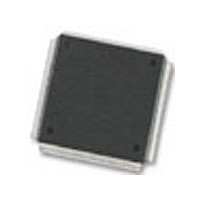
MC68376BAMFT20 Freescale Semiconductor, MC68376BAMFT20 Datasheet - Page 388

MC68376BAMFT20
Manufacturer Part Number
MC68376BAMFT20
Description
Manufacturer
Freescale Semiconductor
Datasheet
1.MC68376BAMFT20.pdf
(434 pages)
Specifications of MC68376BAMFT20
Cpu Family
68K/M683xx
Device Core
ColdFire
Device Core Size
32b
Frequency (max)
20MHz
Interface Type
QSPI/SCI
Program Memory Type
ROM
Program Memory Size
8KB
Total Internal Ram Size
7.5KB
# I/os (max)
18
Number Of Timers - General Purpose
2
Operating Supply Voltage (typ)
5V
Operating Supply Voltage (max)
5.25V
Operating Supply Voltage (min)
4.75V
On-chip Adc
16-chx10-bit
Instruction Set Architecture
RISC
Operating Temp Range
-40C to 125C
Operating Temperature Classification
Automotive
Mounting
Surface Mount
Pin Count
160
Package Type
PQFP
Lead Free Status / Rohs Status
Not Compliant
Available stocks
Company
Part Number
Manufacturer
Quantity
Price
Company:
Part Number:
MC68376BAMFT20
Manufacturer:
FREESCAL
Quantity:
245
- Current page: 388 of 434
- Download datasheet (7Mb)
EN — PWMSM Enable
CLK[2:0] — Clock Rate Selection
D-70
MOTOROLA
This control bit enables and disables the PWMSM.
While the PWMSM is disabled (EN = 0):
When the EN bit is changed from zero to one:
While EN is set, the PWMSM continuously generates a pulse width modulated output
signal based on the data in PWMA2 and PWMB2 which are updated via PWMA1 and
PWMB2 each time a period is completed.
The CLK[2:0] bits select one of the eight counter clock sources coming from the
PWMSM prescaler. These bits can be changed at any time. Table D-50 shows the
counter clock sources and rates in detail.
0 = Disable the PWMSM.
1 = Enable the PWMSM.
• The output flip-flop is held in reset and the level on the output pin is set to one or
• The PWMSM divide-by-256 prescaler is held in reset.
• The counter stops incrementing and is at $0001.
• The comparators are disabled.
• The PWMA1 and PWMB1 registers permanently transfer their contents to the
• The output flip-flop is set to start the first pulse.
• The PWMSM divide-by-256 prescaler is released.
• The counter is released and starts to increment from $0001.
• The FLAG bit is set to indicate that PWMA1 and PWMB1 can be updated with
zero according to the state of the POL bit.
buffer registers PWMA2 and PWMB2, respectively.
new values.
POL
0
1
0
1
To prevent unwanted output waveform glitches when disabling the
PWMSM, first write to PWMB1 to generate one period of 0% duty
cycle, then clear EN.
EN
0
0
1
1
Table D-49 PWMSM Output Pin Polarity Selection
Output Pin State
Always high
Always low
High pulse
Low pulse
REGISTER SUMMARY
Periodic Edge Variable Edge Optional Interrupt On
Falling edge
Rising edge
—
—
NOTE
Falling edge
Rising edge
—
—
Falling edge
Rising edge
—
—
USER’S MANUAL
MC68336/376
Related parts for MC68376BAMFT20
Image
Part Number
Description
Manufacturer
Datasheet
Request
R
Part Number:
Description:
Manufacturer:
Freescale Semiconductor, Inc
Datasheet:
Part Number:
Description:
Manufacturer:
Freescale Semiconductor, Inc
Datasheet:
Part Number:
Description:
Manufacturer:
Freescale Semiconductor, Inc
Datasheet:
Part Number:
Description:
Manufacturer:
Freescale Semiconductor, Inc
Datasheet:
Part Number:
Description:
Manufacturer:
Freescale Semiconductor, Inc
Datasheet:
Part Number:
Description:
Manufacturer:
Freescale Semiconductor, Inc
Datasheet:
Part Number:
Description:
Manufacturer:
Freescale Semiconductor, Inc
Datasheet:
Part Number:
Description:
Manufacturer:
Freescale Semiconductor, Inc
Datasheet:
Part Number:
Description:
Manufacturer:
Freescale Semiconductor, Inc
Datasheet:
Part Number:
Description:
Manufacturer:
Freescale Semiconductor, Inc
Datasheet:
Part Number:
Description:
Manufacturer:
Freescale Semiconductor, Inc
Datasheet:
Part Number:
Description:
Manufacturer:
Freescale Semiconductor, Inc
Datasheet:
Part Number:
Description:
Manufacturer:
Freescale Semiconductor, Inc
Datasheet:
Part Number:
Description:
Manufacturer:
Freescale Semiconductor, Inc
Datasheet:
Part Number:
Description:
Manufacturer:
Freescale Semiconductor, Inc
Datasheet:


