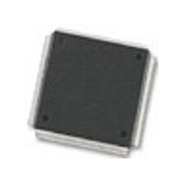
MC68376BAMFT20 Freescale Semiconductor, MC68376BAMFT20 Datasheet - Page 140

MC68376BAMFT20
Manufacturer Part Number
MC68376BAMFT20
Description
Manufacturer
Freescale Semiconductor
Datasheet
1.MC68376BAMFT20.pdf
(434 pages)
Specifications of MC68376BAMFT20
Cpu Family
68K/M683xx
Device Core
ColdFire
Device Core Size
32b
Frequency (max)
20MHz
Interface Type
QSPI/SCI
Program Memory Type
ROM
Program Memory Size
8KB
Total Internal Ram Size
7.5KB
# I/os (max)
18
Number Of Timers - General Purpose
2
Operating Supply Voltage (typ)
5V
Operating Supply Voltage (max)
5.25V
Operating Supply Voltage (min)
4.75V
On-chip Adc
16-chx10-bit
Instruction Set Architecture
RISC
Operating Temp Range
-40C to 125C
Operating Temperature Classification
Automotive
Mounting
Surface Mount
Pin Count
160
Package Type
PQFP
Lead Free Status / Rohs Status
Not Compliant
Available stocks
Company
Part Number
Manufacturer
Quantity
Price
Company:
Part Number:
MC68376BAMFT20
Manufacturer:
FREESCAL
Quantity:
245
- Current page: 140 of 434
- Download datasheet (7Mb)
5.9.4 Chip-Select Reset Operation
5-62
MOTOROLA
Because address match logic functions only after the EBI transfers an interrupt ac-
knowledge cycle to the external address bus following IARB contention, chip-select
logic generates AVEC or DSACK signals only in response to interrupt requests from
external IRQ pins. If an internal module makes an interrupt request of a certain priority,
and the chip-select base address and option registers are programmed to generate
AVEC or DSACK signals in response to an interrupt acknowledge cycle for that priority
level, chip-select logic does not respond to the interrupt acknowledge cycle, and the
internal module supplies a vector number and generates an internal DSACK signal to
terminate the cycle.
Perform the following operations before using a chip-select to generate an interrupt
acknowledge signal:
The least significant bit of each of the 2-bit chip-select pin assignment fields in
CSPAR0 and CSPAR1 each have a reset value of one. The reset values of the most
significant bits of each field are determined by the states of DATA[7:1] during reset.
There are weak internal pull-up drivers for each of the data lines so that chip-select
operation is selected by default out of reset. However, the internal pull-up drivers can
be overcome by bus loading effects.
To ensure a particular configuration out of reset, use an active device to put the data
lines in a known state during reset. The base address fields in chip-select base ad-
dress registers CSBAR[0:10] and chip-select option registers CSOR[0:10] have the re-
set values shown in Table 5-21. The BYTE fields of CSOR[0:10] have a reset value of
“disable”, so that a chip-select signal cannot be asserted until the base and option reg-
isters are initialized.
1. Program the base address field to all ones.
2. Program block size to no more than 64 Kbytes, so that the address comparator
3. Set the R/W field to read only. An interrupt acknowledge cycle is performed as
4. Set the BYTE field to lower byte when using a 16-bit port, as the external vector
If an interrupting device does not provide a vector number, an autovector acknowl-
edge must be generated, either by asserting the AVEC pin or by generating AVEC
internally using the chip-select option register. This terminates the bus cycle.
checks ADDR[19:16] against the corresponding bits in the base address regis-
ter. (The CPU32 places the CPU space bus cycle type on ADDR[19:16].)
a read cycle.
for a 16-bit port is fetched from the lower byte. Set the BYTE field to upper byte
when using an 8-bit port.
SYSTEM INTEGRATION MODULE
USER’S MANUAL
MC68336/376
Related parts for MC68376BAMFT20
Image
Part Number
Description
Manufacturer
Datasheet
Request
R
Part Number:
Description:
Manufacturer:
Freescale Semiconductor, Inc
Datasheet:
Part Number:
Description:
Manufacturer:
Freescale Semiconductor, Inc
Datasheet:
Part Number:
Description:
Manufacturer:
Freescale Semiconductor, Inc
Datasheet:
Part Number:
Description:
Manufacturer:
Freescale Semiconductor, Inc
Datasheet:
Part Number:
Description:
Manufacturer:
Freescale Semiconductor, Inc
Datasheet:
Part Number:
Description:
Manufacturer:
Freescale Semiconductor, Inc
Datasheet:
Part Number:
Description:
Manufacturer:
Freescale Semiconductor, Inc
Datasheet:
Part Number:
Description:
Manufacturer:
Freescale Semiconductor, Inc
Datasheet:
Part Number:
Description:
Manufacturer:
Freescale Semiconductor, Inc
Datasheet:
Part Number:
Description:
Manufacturer:
Freescale Semiconductor, Inc
Datasheet:
Part Number:
Description:
Manufacturer:
Freescale Semiconductor, Inc
Datasheet:
Part Number:
Description:
Manufacturer:
Freescale Semiconductor, Inc
Datasheet:
Part Number:
Description:
Manufacturer:
Freescale Semiconductor, Inc
Datasheet:
Part Number:
Description:
Manufacturer:
Freescale Semiconductor, Inc
Datasheet:
Part Number:
Description:
Manufacturer:
Freescale Semiconductor, Inc
Datasheet:


