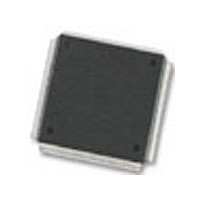
MC68376BAMFT20 Freescale Semiconductor, MC68376BAMFT20 Datasheet - Page 270

MC68376BAMFT20
Manufacturer Part Number
MC68376BAMFT20
Description
Manufacturer
Freescale Semiconductor
Datasheet
1.MC68376BAMFT20.pdf
(434 pages)
Specifications of MC68376BAMFT20
Cpu Family
68K/M683xx
Device Core
ColdFire
Device Core Size
32b
Frequency (max)
20MHz
Interface Type
QSPI/SCI
Program Memory Type
ROM
Program Memory Size
8KB
Total Internal Ram Size
7.5KB
# I/os (max)
18
Number Of Timers - General Purpose
2
Operating Supply Voltage (typ)
5V
Operating Supply Voltage (max)
5.25V
Operating Supply Voltage (min)
4.75V
On-chip Adc
16-chx10-bit
Instruction Set Architecture
RISC
Operating Temp Range
-40C to 125C
Operating Temperature Classification
Automotive
Mounting
Surface Mount
Pin Count
160
Package Type
PQFP
Lead Free Status / Rohs Status
Not Compliant
Available stocks
Company
Part Number
Manufacturer
Quantity
Price
Company:
Part Number:
MC68376BAMFT20
Manufacturer:
FREESCAL
Quantity:
245
- Current page: 270 of 434
- Download datasheet (7Mb)
13.5.4.1 Receive Message Buffer Deactivation
13-14
MOTOROLA
The user should read a received frame from its message buffer in the following order:
If a read of the free running timer is not performed, that message buffer remains locked
until the read process starts for another message buffer. Only a single message buffer
is locked at a time. When reading a received message, the only mandatory read op-
eration is that of the control/status word. This assures data coherency.
If the BUSY bit is set in the message buffer code, the CPU32 should defer accessing
that buffer until this bit is negated. Refer to Table 13-2.
Because the received identifier field is always stored in the matching receive message
buffer, the contents of the identifier field in a receive message buffer may change if
one or more of the ID bits are masked.
Any write access to the control/status word of a receive message buffer during the pro-
cess of selecting a message buffer for reception immediately deactivates that mes-
sage buffer, removing it from the reception process.
If a receive message buffer is deactivated while a message is being transferred into it,
the transfer is halted and no interrupt is requested. If this occurs, that receive message
buffer may contain mixed data from two different frames.
Data should never be written into a receive message buffer. If this is done while a mes-
sage is being transferred from a serial message buffer, the control/status word will re-
flect a full or overrun condition, but no interrupt will be requested.
1. The frame is transferred to the first (lowest entry) matching receive message
2. The value of the free-running timer (captured at the beginning of the identifier
3. The ID field, data field and RX length field are stored.
4. The code field is updated.
5. The status flag is set in the IFLAG register.
1. Control/status word (mandatory, as it activates the internal lock for this buffer)
2. ID (optional, since it is needed only if a mask was used)
3. Data field word(s)
4. Free-running timer (optional, as it releases the internal lock)
buffer.
field on the CAN bus) is written into the time stamp field in the message buffer.
The CPU32 should check the status of a message buffer by reading
the status flag in the IFLAG register and not by reading the control/
status word code field for that message buffer. This prevents the
buffer from being locked inadvertently.
CAN 2.0B CONTROLLER MODULE (TouCAN)
NOTE
USER’S MANUAL
MC68336/376
Related parts for MC68376BAMFT20
Image
Part Number
Description
Manufacturer
Datasheet
Request
R
Part Number:
Description:
Manufacturer:
Freescale Semiconductor, Inc
Datasheet:
Part Number:
Description:
Manufacturer:
Freescale Semiconductor, Inc
Datasheet:
Part Number:
Description:
Manufacturer:
Freescale Semiconductor, Inc
Datasheet:
Part Number:
Description:
Manufacturer:
Freescale Semiconductor, Inc
Datasheet:
Part Number:
Description:
Manufacturer:
Freescale Semiconductor, Inc
Datasheet:
Part Number:
Description:
Manufacturer:
Freescale Semiconductor, Inc
Datasheet:
Part Number:
Description:
Manufacturer:
Freescale Semiconductor, Inc
Datasheet:
Part Number:
Description:
Manufacturer:
Freescale Semiconductor, Inc
Datasheet:
Part Number:
Description:
Manufacturer:
Freescale Semiconductor, Inc
Datasheet:
Part Number:
Description:
Manufacturer:
Freescale Semiconductor, Inc
Datasheet:
Part Number:
Description:
Manufacturer:
Freescale Semiconductor, Inc
Datasheet:
Part Number:
Description:
Manufacturer:
Freescale Semiconductor, Inc
Datasheet:
Part Number:
Description:
Manufacturer:
Freescale Semiconductor, Inc
Datasheet:
Part Number:
Description:
Manufacturer:
Freescale Semiconductor, Inc
Datasheet:
Part Number:
Description:
Manufacturer:
Freescale Semiconductor, Inc
Datasheet:


