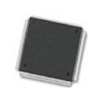
MC68376BAMFT20 Freescale Semiconductor, MC68376BAMFT20 Datasheet - Page 106

MC68376BAMFT20
Manufacturer Part Number
MC68376BAMFT20
Description
Manufacturer
Freescale Semiconductor
Datasheet
1.MC68376BAMFT20.pdf
(434 pages)
Specifications of MC68376BAMFT20
Cpu Family
68K/M683xx
Device Core
ColdFire
Device Core Size
32b
Frequency (max)
20MHz
Interface Type
QSPI/SCI
Program Memory Type
ROM
Program Memory Size
8KB
Total Internal Ram Size
7.5KB
# I/os (max)
18
Number Of Timers - General Purpose
2
Operating Supply Voltage (typ)
5V
Operating Supply Voltage (max)
5.25V
Operating Supply Voltage (min)
4.75V
On-chip Adc
16-chx10-bit
Instruction Set Architecture
RISC
Operating Temp Range
-40C to 125C
Operating Temperature Classification
Automotive
Mounting
Surface Mount
Pin Count
160
Package Type
PQFP
Lead Free Status / Rohs Status
Not Compliant
Available stocks
Company
Part Number
Manufacturer
Quantity
Price
Company:
Part Number:
MC68376BAMFT20
Manufacturer:
FREESCAL
Quantity:
245
- Current page: 106 of 434
- Download datasheet (7Mb)
5.6.2.1 Read Cycle
5-28
MOTOROLA
If bus termination signals remain unasserted, the MCU will continue to insert wait
states, and the bus cycle will never end. If no peripheral responds to an access, or if
an access is invalid, external logic should assert the BERR or HALT signals to abort
the bus cycle (when BERR and HALT are asserted simultaneously, the CPU32 acts
as though only BERR is asserted). When enabled, the SIM bus monitor asserts BERR
when DSACK response time exceeds a predetermined limit. The bus monitor timeout
period is determined by the BMT[1:0] field in SYPCR. The maximum bus monitor tim-
eout period is 64 system clock cycles.
During a read cycle, the MCU transfers data from an external memory or peripheral
device. If the instruction specifies a long-word or word operation, the MCU attempts to
read two bytes at once. For a byte operation, the MCU reads one byte. The portion of
the data bus from which each byte is read depends on operand size, peripheral ad-
dress, and peripheral port size. Figure 5-10 is a flowchart of a word read cycle. Refer
to 5.5.2 Dynamic Bus Sizing, 5.5.4 Misaligned Operands, and the SIM Reference
Manual (SIMRM/AD) for more information.
1) SET R/W TO READ
2) DRIVE ADDRESS ON ADDR[23:0]
3) DRIVE FUNCTION CODE ON FC[2:0]
4) DRIVE SIZ[1:0] FOR OPERAND SIZE
NEGATE AS AND DS (S5)
ASSERT AS AND DS (S1)
START NEXT CYCLE (S0)
ADDRESS DEVICE (S0)
DECODE DSACK (S3)
LATCH DATA (S4)
Figure 5-10 Word Read Cycle Flowchart
MCU
SYSTEM INTEGRATION MODULE
1) DECODE ADDR, R/W, SIZ[1:0], DS
2) PLACE DATA ON DATA[15:0] OR
3) DRIVE DSACK SIGNALS
1) REMOVE DATA FROM DATA BUS
2) NEGATE DSACK
DATA[15:8] IF 8-BIT DATA
TERMINATE CYCLE (S5)
PRESENT DATA (S2)
PERIPHERAL
USER’S MANUAL
MC68336/376
RD CYC FLOW
Related parts for MC68376BAMFT20
Image
Part Number
Description
Manufacturer
Datasheet
Request
R
Part Number:
Description:
Manufacturer:
Freescale Semiconductor, Inc
Datasheet:
Part Number:
Description:
Manufacturer:
Freescale Semiconductor, Inc
Datasheet:
Part Number:
Description:
Manufacturer:
Freescale Semiconductor, Inc
Datasheet:
Part Number:
Description:
Manufacturer:
Freescale Semiconductor, Inc
Datasheet:
Part Number:
Description:
Manufacturer:
Freescale Semiconductor, Inc
Datasheet:
Part Number:
Description:
Manufacturer:
Freescale Semiconductor, Inc
Datasheet:
Part Number:
Description:
Manufacturer:
Freescale Semiconductor, Inc
Datasheet:
Part Number:
Description:
Manufacturer:
Freescale Semiconductor, Inc
Datasheet:
Part Number:
Description:
Manufacturer:
Freescale Semiconductor, Inc
Datasheet:
Part Number:
Description:
Manufacturer:
Freescale Semiconductor, Inc
Datasheet:
Part Number:
Description:
Manufacturer:
Freescale Semiconductor, Inc
Datasheet:
Part Number:
Description:
Manufacturer:
Freescale Semiconductor, Inc
Datasheet:
Part Number:
Description:
Manufacturer:
Freescale Semiconductor, Inc
Datasheet:
Part Number:
Description:
Manufacturer:
Freescale Semiconductor, Inc
Datasheet:
Part Number:
Description:
Manufacturer:
Freescale Semiconductor, Inc
Datasheet:


