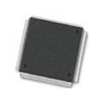
MC68376BAMFT20 Freescale Semiconductor, MC68376BAMFT20 Datasheet - Page 190

MC68376BAMFT20
Manufacturer Part Number
MC68376BAMFT20
Description
Manufacturer
Freescale Semiconductor
Datasheet
1.MC68376BAMFT20.pdf
(434 pages)
Specifications of MC68376BAMFT20
Cpu Family
68K/M683xx
Device Core
ColdFire
Device Core Size
32b
Frequency (max)
20MHz
Interface Type
QSPI/SCI
Program Memory Type
ROM
Program Memory Size
8KB
Total Internal Ram Size
7.5KB
# I/os (max)
18
Number Of Timers - General Purpose
2
Operating Supply Voltage (typ)
5V
Operating Supply Voltage (max)
5.25V
Operating Supply Voltage (min)
4.75V
On-chip Adc
16-chx10-bit
Instruction Set Architecture
RISC
Operating Temp Range
-40C to 125C
Operating Temperature Classification
Automotive
Mounting
Surface Mount
Pin Count
160
Package Type
PQFP
Lead Free Status / Rohs Status
Not Compliant
Available stocks
Company
Part Number
Manufacturer
Quantity
Price
Company:
Part Number:
MC68376BAMFT20
Manufacturer:
FREESCAL
Quantity:
245
- Current page: 190 of 434
- Download datasheet (7Mb)
8.6.4 Interrupt Arbitration Priority
8.7 Test Register
8.8 General-Purpose I/O Port Operation
8-8
MOTOROLA
data space accesses. The SUPV bit in QADCMCR designates the assignable space
as supervisor or unrestricted.
Attempts to read supervisor-only data space when the CPU32 is not in supervisor
mode causes a value of $0000 to be returned. Attempts to read assignable data space
when the CPU32 is not in supervisor mode and when the space is programmed as
supervisor space, causes a value of $FFFF to be returned. Attempts to write supervi-
sor-only or supervisor-assigned data space when the CPU32 is in user mode has no
effect.
The supervisor-only data space segment contains the QADC global registers, which
include QADCMCR, QADCTEST, and QADCINT. The supervisor/unrestricted space
designation for the CCW table, the result word table, and the remaining QADC
registers is programmable. Refer to D.5.1 QADC Module Configuration Register for
more information.
Each module that can request interrupts, including the QADC, has an interrupt arbitra-
tion number (IARB) field in its module configuration register. Each IARB field must
have a different non-zero value. During an interrupt acknowledge cycle, IARB permits
arbitration among simultaneous interrupts of the same priority level.
The reset value of IARB in the QADCMCR is $0. Initialization software must set the
IARB field to a non-zero value in order for QADC interrupts to be arbitrated. Refer to
D.5.1 QADC Module Configuration Register for more information.
The QADC test register (QADCTEST) is used only during factory testing of the MCU.
QADC port pins, when used as general-purpose input, are conditioned by a synchro-
nizer with an enable feature. The synchronizer is not enabled until the QADC decodes
an IMB bus cycle which addresses the port data register to minimize the high-current
effect of mid-level signals on the inputs used for analog signals. Digital input signals
must meet the input low voltage (V
PENDIX A ELECTRICAL CHARACTERISTICS. If an analog input pin does not meet
the digital input pin specifications when a digital port read operation occurs, an inde-
terminate state is read.
During a port data register read, the actual value of the pin is reported when its corre-
sponding bit in the data direction register defines the pin to be an input (port A only).
When the data direction bit specifies the pin to be an output, the content of the port
data register is read. By reading the latch which drives the output pin, software instruc-
tions that read data, modify it, and write the result, like bit manipulation instructions,
work correctly.
QUEUED ANALOG-TO-DIGITAL CONVERTER MODULE
IL
) or input high voltage (V
IH
) specifications in AP-
USER’S MANUAL
MC68336/376
Related parts for MC68376BAMFT20
Image
Part Number
Description
Manufacturer
Datasheet
Request
R
Part Number:
Description:
Manufacturer:
Freescale Semiconductor, Inc
Datasheet:
Part Number:
Description:
Manufacturer:
Freescale Semiconductor, Inc
Datasheet:
Part Number:
Description:
Manufacturer:
Freescale Semiconductor, Inc
Datasheet:
Part Number:
Description:
Manufacturer:
Freescale Semiconductor, Inc
Datasheet:
Part Number:
Description:
Manufacturer:
Freescale Semiconductor, Inc
Datasheet:
Part Number:
Description:
Manufacturer:
Freescale Semiconductor, Inc
Datasheet:
Part Number:
Description:
Manufacturer:
Freescale Semiconductor, Inc
Datasheet:
Part Number:
Description:
Manufacturer:
Freescale Semiconductor, Inc
Datasheet:
Part Number:
Description:
Manufacturer:
Freescale Semiconductor, Inc
Datasheet:
Part Number:
Description:
Manufacturer:
Freescale Semiconductor, Inc
Datasheet:
Part Number:
Description:
Manufacturer:
Freescale Semiconductor, Inc
Datasheet:
Part Number:
Description:
Manufacturer:
Freescale Semiconductor, Inc
Datasheet:
Part Number:
Description:
Manufacturer:
Freescale Semiconductor, Inc
Datasheet:
Part Number:
Description:
Manufacturer:
Freescale Semiconductor, Inc
Datasheet:
Part Number:
Description:
Manufacturer:
Freescale Semiconductor, Inc
Datasheet:


