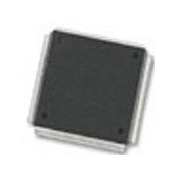
MC68376BAMFT20 Freescale Semiconductor, MC68376BAMFT20 Datasheet - Page 282

MC68376BAMFT20
Manufacturer Part Number
MC68376BAMFT20
Description
Manufacturer
Freescale Semiconductor
Datasheet
1.MC68376BAMFT20.pdf
(434 pages)
Specifications of MC68376BAMFT20
Cpu Family
68K/M683xx
Device Core
ColdFire
Device Core Size
32b
Frequency (max)
20MHz
Interface Type
QSPI/SCI
Program Memory Type
ROM
Program Memory Size
8KB
Total Internal Ram Size
7.5KB
# I/os (max)
18
Number Of Timers - General Purpose
2
Operating Supply Voltage (typ)
5V
Operating Supply Voltage (max)
5.25V
Operating Supply Voltage (min)
4.75V
On-chip Adc
16-chx10-bit
Instruction Set Architecture
RISC
Operating Temp Range
-40C to 125C
Operating Temperature Classification
Automotive
Mounting
Surface Mount
Pin Count
160
Package Type
PQFP
Lead Free Status / Rohs Status
Not Compliant
Available stocks
Company
Part Number
Manufacturer
Quantity
Price
Company:
Part Number:
MC68376BAMFT20
Manufacturer:
FREESCAL
Quantity:
245
- Current page: 282 of 434
- Download datasheet (7Mb)
NOTES:
A-6
10. This parameter is periodically sampled rather than 100% tested.
MOTOROLA
1. Applies to :
2. Input-Only Pins: EXTAL, TSTME/TSC, BKPT, PAI, T2CLK, RXD, CTM2C
3. Does not apply to HALT and RESET because they are open drain pins. Does not apply to port QS[7:0] (TXD,
4. Use of an active pulldown device is recommended.
5. Total operating current is the sum of the appropriate I
6. Current measured at maximum system clock frequency, all modules active.
7. The SRAM module will not switch into standby mode as long as V
8. When V
9. Power dissipation measured at system clock frequency, all modules active. Power dissipation can be calculated us-
Output-Only Pins: CSBOOT, BG/CS, CLKOUT, FREEZE/QUOT, IPIPE
Input/Output Pins:
Pin groups do not include QADC pins. See Tables A-11 through A-14 for information concerning the QADC.
PCS[3:1], PCS0/SS, SCK, MOSI, MISO) in wired-OR mode.
currents for device modules powered by V
volts. The SRAM array cannot be accessed while the module is in standby mode.
the V
specification. System noise on the V
ing the following expression:
STBY
DD
and V
is transitioning during power-up or power down sequence, and V
Port E[7:4] — SIZ[1:0], AS, DS
Port F[7:0] — IRQ[7:1], MODCLK
Port QS[7:0] — TXD, PCS[3:1], PCS0/SS, SCK, MOSI, MISO
TPUCH[15:0], T2CLK, CPWM[8:5], CTD[4:3], CTD[10:9], CTM2C
BKPT/DSCLK, IFETCH, RESET, RXD, TSTME/TSC
EXTAL (when PLL enabled)
Group 1: DATA[15:0], IFETCH, TPUCH[15:0], CPWM[8:5], CTD[4:3], CTD[10:9]
Group 2: Port C[6:0] — ADDR[22:19]/CS[9:6], FC[2:0]/CS[5:3]
ADDR23/CS10/ECLK, ADDR[18:0], R/W, BERR, BR/CS0, BGACK/CS2
Group 3: HALT, RESET
Group 4: MISO, MOSI, SCK
Port E[7:0] — SIZ[1:0], AS, DS, AVEC, RMC, DSACK[1:0]
Port F[7:0] — IRQ[7:1], MODCLK
Port QS[7:3] — TXD, PCS[3:1], PCS0/SS
DD
pins, which causes standby current to increase toward the maximum transient condition
P
D
ELECTRICAL CHARACTERISTICS
= Maximum V
DD
and V
DDE
STBY
and V
DD
pins can contribute to this condition.
(Run I
DDI
DD
, I
pins.
DD
DDSYN
+ I
DDSYN
, and I
SB
does not exceed V
+ I
SB
SB
values. I
) + Maximum V
SB
is applied, current flows between
DD
values include supply
DD
DDA
by more than 0.5
USER’S MANUAL
(I
DDA
MC68336/376
)
Related parts for MC68376BAMFT20
Image
Part Number
Description
Manufacturer
Datasheet
Request
R
Part Number:
Description:
Manufacturer:
Freescale Semiconductor, Inc
Datasheet:
Part Number:
Description:
Manufacturer:
Freescale Semiconductor, Inc
Datasheet:
Part Number:
Description:
Manufacturer:
Freescale Semiconductor, Inc
Datasheet:
Part Number:
Description:
Manufacturer:
Freescale Semiconductor, Inc
Datasheet:
Part Number:
Description:
Manufacturer:
Freescale Semiconductor, Inc
Datasheet:
Part Number:
Description:
Manufacturer:
Freescale Semiconductor, Inc
Datasheet:
Part Number:
Description:
Manufacturer:
Freescale Semiconductor, Inc
Datasheet:
Part Number:
Description:
Manufacturer:
Freescale Semiconductor, Inc
Datasheet:
Part Number:
Description:
Manufacturer:
Freescale Semiconductor, Inc
Datasheet:
Part Number:
Description:
Manufacturer:
Freescale Semiconductor, Inc
Datasheet:
Part Number:
Description:
Manufacturer:
Freescale Semiconductor, Inc
Datasheet:
Part Number:
Description:
Manufacturer:
Freescale Semiconductor, Inc
Datasheet:
Part Number:
Description:
Manufacturer:
Freescale Semiconductor, Inc
Datasheet:
Part Number:
Description:
Manufacturer:
Freescale Semiconductor, Inc
Datasheet:
Part Number:
Description:
Manufacturer:
Freescale Semiconductor, Inc
Datasheet:


