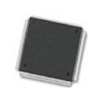
MC68376BAMFT20 Freescale Semiconductor, MC68376BAMFT20 Datasheet - Page 178

MC68376BAMFT20
Manufacturer Part Number
MC68376BAMFT20
Description
Manufacturer
Freescale Semiconductor
Datasheet
1.MC68376BAMFT20.pdf
(434 pages)
Specifications of MC68376BAMFT20
Cpu Family
68K/M683xx
Device Core
ColdFire
Device Core Size
32b
Frequency (max)
20MHz
Interface Type
QSPI/SCI
Program Memory Type
ROM
Program Memory Size
8KB
Total Internal Ram Size
7.5KB
# I/os (max)
18
Number Of Timers - General Purpose
2
Operating Supply Voltage (typ)
5V
Operating Supply Voltage (max)
5.25V
Operating Supply Voltage (min)
4.75V
On-chip Adc
16-chx10-bit
Instruction Set Architecture
RISC
Operating Temp Range
-40C to 125C
Operating Temperature Classification
Automotive
Mounting
Surface Mount
Pin Count
160
Package Type
PQFP
Lead Free Status / Rohs Status
Not Compliant
Available stocks
Company
Part Number
Manufacturer
Quantity
Price
Company:
Part Number:
MC68376BAMFT20
Manufacturer:
FREESCAL
Quantity:
245
- Current page: 178 of 434
- Download datasheet (7Mb)
9.4.3.6 Receiver Operation
9.4.3.7 Idle-Line Detection
9-28
MOTOROLA
The RE bit in SCCR1 enables (RE = 1) and disables (RE = 0) the receiver. The
receiver contains a receive serial shifter and a parallel receive data register (RDR) lo-
cated in the SCI data register (SCDR). The serial shifter cannot be directly accessed
by the CPU32. The receiver is double-buffered, allowing data to be held in the RDR
while other data is shifted in.
Receiver bit processor logic drives a state machine that determines the logic level for
each bit-time. This state machine controls when the bit processor logic is to sample
the RXD pin and also controls when data is to be passed to the receive serial shifter.
A receive time clock is used to control sampling and synchronization. Data is shifted
into the receive serial shifter according to the most recent synchronization of the re-
ceive time clock with the incoming data stream. From this point on, data movement is
synchronized with the MCU system clock. Operation of the receiver state machine is
detailed in the QSM Reference Manual (QSMRM/AD).
The number of bits shifted in by the receiver depends on the serial format. However,
all frames must end with at least one stop bit. When the stop bit is received, the frame
is considered to be complete, and the received data in the serial shifter is transferred
to the RDR. The receiver data register flag (RDRF) is set when the data is transferred.
Noise errors, parity errors, and framing errors can be detected while a data stream is
being received. Although error conditions are detected as bits are received, the noise
flag (NF), the parity flag (PF), and the framing error (FE) flag in SCSR are not set until
data is transferred from the serial shifter to the RDR.
RDRF must be cleared before the next transfer from the shifter can take place. If
RDRF is set when the shifter is full, transfers are inhibited and the overrun error (OR)
flag in SCSR is set. OR indicates that the RDR needs to be serviced faster. When OR
is set, the data in the RDR is preserved, but the data in the serial shifter is lost. Be-
cause framing, noise, and parity errors are detected while data is in the serial shifter,
FE, NF, and PF cannot occur at the same time as OR.
When the CPU32 reads SCSR and SCDR in sequence, it acquires status and data,
and also clears the status flags. Reading SCSR acquires status and arms the clearing
mechanism. Reading SCDR acquires data and clears SCSR.
When RIE in SCCR1 is set, an interrupt request is generated whenever RDRF is set.
Because receiver status flags are set at the same time as RDRF, they do not have
separate interrupt enables.
During a typical serial transmission, frames are transmitted isochronally and no idle
time occurs between frames. Even when all the data bits in a frame are logic ones, the
start bit provides one logic zero bit-time during the frame. An idle line is a sequence of
contiguous ones equal to the current frame size. Frame size is determined by the state
of the M bit in SCCR1.
QUEUED SERIAL MODULE
USER’S MANUAL
MC68336/376
Related parts for MC68376BAMFT20
Image
Part Number
Description
Manufacturer
Datasheet
Request
R
Part Number:
Description:
Manufacturer:
Freescale Semiconductor, Inc
Datasheet:
Part Number:
Description:
Manufacturer:
Freescale Semiconductor, Inc
Datasheet:
Part Number:
Description:
Manufacturer:
Freescale Semiconductor, Inc
Datasheet:
Part Number:
Description:
Manufacturer:
Freescale Semiconductor, Inc
Datasheet:
Part Number:
Description:
Manufacturer:
Freescale Semiconductor, Inc
Datasheet:
Part Number:
Description:
Manufacturer:
Freescale Semiconductor, Inc
Datasheet:
Part Number:
Description:
Manufacturer:
Freescale Semiconductor, Inc
Datasheet:
Part Number:
Description:
Manufacturer:
Freescale Semiconductor, Inc
Datasheet:
Part Number:
Description:
Manufacturer:
Freescale Semiconductor, Inc
Datasheet:
Part Number:
Description:
Manufacturer:
Freescale Semiconductor, Inc
Datasheet:
Part Number:
Description:
Manufacturer:
Freescale Semiconductor, Inc
Datasheet:
Part Number:
Description:
Manufacturer:
Freescale Semiconductor, Inc
Datasheet:
Part Number:
Description:
Manufacturer:
Freescale Semiconductor, Inc
Datasheet:
Part Number:
Description:
Manufacturer:
Freescale Semiconductor, Inc
Datasheet:
Part Number:
Description:
Manufacturer:
Freescale Semiconductor, Inc
Datasheet:


