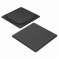
DS33R41+ Maxim Integrated Products, DS33R41+ Datasheet - Page 68

DS33R41+
Manufacturer Part Number
DS33R41+
Description
IC TXRX ETHERNET MAP 400-BGA
Manufacturer
Maxim Integrated Products
Type
Transceiverr
Datasheet
1.DS33R41.pdf
(335 pages)
Specifications of DS33R41+
Number Of Drivers/receivers
4/4
Protocol
T1/E1/J1
Voltage - Supply
3.14 V ~ 3.47 V
Mounting Type
Surface Mount
Package / Case
400-BGA
Lead Free Status / RoHS Status
Lead free / RoHS Compliant
- Current page: 68 of 335
- Download datasheet (2Mb)
10 INTEGRATED T1/E1/J1 TRANSCEIVERS
10.1 T1/E1/J1 Transceiver Clocks
The device contains an on-chip clock synthesizer that generates a user-selectable clock referenced to the
recovered receive clock (RCLK). The synthesizer uses a phase-locked loop to generate low-jitter clocks. Common
applications include generation of port and backplane system clocks.
Figure 10-1
the various loopback modes and jitter attenuator positions. Although there is only one jitter attenuator, which can
be placed in the receive or transmit path, two are shown for simplification and clarity.
Figure 10-1. Transceiver Clock Structure
The TCLKT MUX is dependent on the state of the TCSS0 and TCSS1 bits in the TR.CCR1 register and the state of
the TCLKT pin.
RXCLK
TXCLK
TO
LIU
shows the clock map of the transceivers. The routing for the transmit and receive clocks are shown for
MCLKS = 0
RCL = 1
RCL = 0
2.048 TO 1.544
SYNTHESIZER
PRE-SCALER
MCLK
LOCAL
LOOPBACK
LLB = 0
LLB = 1
MCLKS = 1
TR.LIC4.MPS0
TR.LIC4.MPS1
TR.LIC2.3
JITTER ATTENUATOR
SEE TR.LIC1
REGISTER
JAS = 0
OR
DJA = 1
JAS = 1
AND
DJA = 0
LTCA
LTCA
JAS = 0
AND
DJA = 0
JAS = 1
OR
DJA = 1
REMOTE
LOOPBACK
RLB = 1
RLB = 0
68 of 335
DJA = 1
DJA = 0
FRAMER
LOOPBACK
FLB = 0
FLB = 1
TRANSMIT
FORMATTER
RECEIVE
FRAMER
8 x PLL
PAYLOAD
LOOPBACK
(SEE NOTES)
PLB = 1
PLB = 0
A
B
BPCLK
SYNTH
C
TCLKT
MUX
TSYSCLK
8XCLK
BPCLK
RCLKO
TCLKT
Related parts for DS33R41+
Image
Part Number
Description
Manufacturer
Datasheet
Request
R

Part Number:
Description:
MAX7528KCWPMaxim Integrated Products [CMOS Dual 8-Bit Buffered Multiplying DACs]
Manufacturer:
Maxim Integrated Products
Datasheet:

Part Number:
Description:
Single +5V, fully integrated, 1.25Gbps laser diode driver.
Manufacturer:
Maxim Integrated Products
Datasheet:

Part Number:
Description:
Single +5V, fully integrated, 155Mbps laser diode driver.
Manufacturer:
Maxim Integrated Products
Datasheet:

Part Number:
Description:
VRD11/VRD10, K8 Rev F 2/3/4-Phase PWM Controllers with Integrated Dual MOSFET Drivers
Manufacturer:
Maxim Integrated Products
Datasheet:

Part Number:
Description:
Highly Integrated Level 2 SMBus Battery Chargers
Manufacturer:
Maxim Integrated Products
Datasheet:

Part Number:
Description:
Current Monitor and Accumulator with Integrated Sense Resistor; ; Temperature Range: -40°C to +85°C
Manufacturer:
Maxim Integrated Products

Part Number:
Description:
TSSOP 14/A�/RS-485 Transceivers with Integrated 100O/120O Termination Resis
Manufacturer:
Maxim Integrated Products

Part Number:
Description:
TSSOP 14/A�/RS-485 Transceivers with Integrated 100O/120O Termination Resis
Manufacturer:
Maxim Integrated Products

Part Number:
Description:
QFN 16/A�/AC-DC and DC-DC Peak-Current-Mode Converters with Integrated Step
Manufacturer:
Maxim Integrated Products

Part Number:
Description:
TDFN/A/65V, 1A, 600KHZ, SYNCHRONOUS STEP-DOWN REGULATOR WITH INTEGRATED SWI
Manufacturer:
Maxim Integrated Products

Part Number:
Description:
Integrated Temperature Controller f
Manufacturer:
Maxim Integrated Products

Part Number:
Description:
SOT23-6/I�/45MHz to 650MHz, Integrated IF VCOs with Differential Output
Manufacturer:
Maxim Integrated Products

Part Number:
Description:
SOT23-6/I�/45MHz to 650MHz, Integrated IF VCOs with Differential Output
Manufacturer:
Maxim Integrated Products

Part Number:
Description:
EVALUATION KIT/2.4GHZ TO 2.5GHZ 802.11G/B RF TRANSCEIVER WITH INTEGRATED PA
Manufacturer:
Maxim Integrated Products

Part Number:
Description:
QFN/E/DUAL PCIE/SATA HIGH SPEED SWITCH WITH INTEGRATED BIAS RESISTOR
Manufacturer:
Maxim Integrated Products
Datasheet:


