DS33R41+ Maxim Integrated Products, DS33R41+ Datasheet - Page 132
DS33R41+
Manufacturer Part Number
DS33R41+
Description
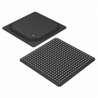
IC TXRX ETHERNET MAP 400-BGA
Manufacturer
Maxim Integrated Products
Type
Transceiverr
Datasheet
1.DS33R41.pdf
(335 pages)
Specifications of DS33R41+
Number Of Drivers/receivers
4/4
Protocol
T1/E1/J1
Voltage - Supply
3.14 V ~ 3.47 V
Mounting Type
Surface Mount
Package / Case
400-BGA
Lead Free Status / RoHS Status
Lead free / RoHS Compliant


Register Name:
Register Description:
Register Address:
Bit #
Name
Default
Bit 2: REF_CLKO OFF (REF_CLKO). This bit determines the REF_CLKO output mode.
Bit 1: INT Pin Mode (INTM). This bit determines the inactive mode of the INT pin. The INT pin always drives low
when active.
Bit 0: Reset (RST). When this bit is set to 1, all of the internal data path and status and control registers (except
this RST bit), on all ports, are reset to their default state. This bit must be set high for a minimum of 100ns.
Register Name:
Register Description:
Register Address:
Bit #
Name
Default
Bit 4: Receive Serial Interface Clock Activity Latched Status 1 (RLCALS1). This bit is set to 1 if the receive
clock for Serial Interface 1 has activity. This bit is cleared upon read.
Bit 0: Transmit Serial Interface Clock Activity Latched Status 1 (TLCALS1). This bit is set to 1 if the transmit
clock for Serial Interface 1 has activity. This bit is cleared upon read.
Bit #
Name
Default
Bit 1: Reference Clock Activity Latched Status (REFCLKS). This bit is set to 1 if REF_CLK has activity. This bit
is cleared upon read.
Bit 0: System Clock Input Latched Status (SYSCLS). This bit is set to 1 if SYSCLKI has activity. This bit is
cleared upon read.
Register Name:
Register Description:
Register Address:
1 = REF_CLKO is disabled and outputs an active low signal.
0 = REF_CLKO is active and in accordance with RMII/MII Selection.
1 = Pin is high impedance when not active.
0 = Pin drives high when not active.
0 = Normal operation.
1 = Reset and force all internal registers to their default values.
—
—
—
7
0
7
0
7
0
—
—
—
6
0
6
0
6
0
GL.RTCAL
Global Receive and Transmit Serial Port Clock Activity Latched Status
04h
GL.SRCALS
Global SDRAM Reference Clock Activity Latched Status
05h
GL.CR1
Global Control Register 1
02h
—
—
—
5
0
5
0
5
0
RLCALS1
132 of 335
—
—
4
0
0
4
0
4
—
—
—
3
0
3
0
3
0
REF_CLKO
—
—
2
0
2
0
0
2
REFCLKS
—
1
0
INTM
1
0
1
0
TLCALS1
SYSCLS
0
0
RST
0
0
0
0
Related parts for DS33R41+
Image
Part Number
Description
Manufacturer
Datasheet
Request
R

Part Number:
Description:
MAX7528KCWPMaxim Integrated Products [CMOS Dual 8-Bit Buffered Multiplying DACs]
Manufacturer:
Maxim Integrated Products
Datasheet:
Part Number:
Description:
Single +5V, fully integrated, 1.25Gbps laser diode driver.
Manufacturer:
Maxim Integrated Products
Datasheet:
Part Number:
Description:
Single +5V, fully integrated, 155Mbps laser diode driver.
Manufacturer:
Maxim Integrated Products
Datasheet:
Part Number:
Description:
VRD11/VRD10, K8 Rev F 2/3/4-Phase PWM Controllers with Integrated Dual MOSFET Drivers
Manufacturer:
Maxim Integrated Products
Datasheet:
Part Number:
Description:
Highly Integrated Level 2 SMBus Battery Chargers
Manufacturer:
Maxim Integrated Products
Datasheet:
Part Number:
Description:
Current Monitor and Accumulator with Integrated Sense Resistor; ; Temperature Range: -40°C to +85°C
Manufacturer:
Maxim Integrated Products
Part Number:
Description:
TSSOP 14/A�/RS-485 Transceivers with Integrated 100O/120O Termination Resis
Manufacturer:
Maxim Integrated Products
Part Number:
Description:
TSSOP 14/A�/RS-485 Transceivers with Integrated 100O/120O Termination Resis
Manufacturer:
Maxim Integrated Products
Part Number:
Description:
QFN 16/A�/AC-DC and DC-DC Peak-Current-Mode Converters with Integrated Step
Manufacturer:
Maxim Integrated Products
Part Number:
Description:
TDFN/A/65V, 1A, 600KHZ, SYNCHRONOUS STEP-DOWN REGULATOR WITH INTEGRATED SWI
Manufacturer:
Maxim Integrated Products
Part Number:
Description:
Integrated Temperature Controller f
Manufacturer:
Maxim Integrated Products
Part Number:
Description:
SOT23-6/I�/45MHz to 650MHz, Integrated IF VCOs with Differential Output
Manufacturer:
Maxim Integrated Products
Part Number:
Description:
SOT23-6/I�/45MHz to 650MHz, Integrated IF VCOs with Differential Output
Manufacturer:
Maxim Integrated Products
Part Number:
Description:
EVALUATION KIT/2.4GHZ TO 2.5GHZ 802.11G/B RF TRANSCEIVER WITH INTEGRATED PA
Manufacturer:
Maxim Integrated Products
Part Number:
Description:
QFN/E/DUAL PCIE/SATA HIGH SPEED SWITCH WITH INTEGRATED BIAS RESISTOR
Manufacturer:
Maxim Integrated Products
Datasheet: