DS33R41+ Maxim Integrated Products, DS33R41+ Datasheet - Page 21
DS33R41+
Manufacturer Part Number
DS33R41+
Description
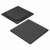
IC TXRX ETHERNET MAP 400-BGA
Manufacturer
Maxim Integrated Products
Type
Transceiverr
Datasheet
1.DS33R41.pdf
(335 pages)
Specifications of DS33R41+
Number Of Drivers/receivers
4/4
Protocol
T1/E1/J1
Voltage - Supply
3.14 V ~ 3.47 V
Mounting Type
Surface Mount
Package / Case
400-BGA
Lead Free Status / RoHS Status
Lead free / RoHS Compliant


7 PIN DESCRIPTIONS
7.1 Pin Functional Description
Note that all digital pins are inout pins in JTAG mode. This feature increases the effectiveness of board level ATPG
patterns.
I = input, O = output, Ipu = input with pullup, Oz = output with tri-state, IO = bidirectional pin, IOz = bidirectional pin with tri-state
Table 7-1. Detailed Pin Descriptions
WR/RW
NAME
RD/DS
D0
D1
D2
D3
D4
D5
D6
D7
A0
A1
A2
A3
A4
A5
A6
A7
A8
A9
DS33R41 Inverse-Multiplexing Ethernet Mapper with Quad Integrated T1/E1/J1 Transceivers
G17
A19
A20
C18
B18
E18
A18
E17
C17
D17
C16
A17
E16
D16
B15
C15
A16
PIN
F17
F16
F15
TYPE
IOZ
IOZ
IOZ
IOZ
IOZ
IOZ
IOZ
IOZ
I
I
I
I
I
I
I
I
I
I
I
I
MICROPROCESSOR PORT
Address Bit 0. Address bit 0 of the microprocessor interface. Least
Significant Bit.
Address Bit 1. Address bit 1 of the microprocessor interface.
Address Bit 2. Address bit 2 of the microprocessor interface.
Address Bit 3. Address bit 3 of the microprocessor interface.
Address Bit 4. Address bit 4 of the microprocessor interface.
Address Bit 5. Address bit 5 of the microprocessor interface.
Address Bit 6. Address bit 6 of the microprocessor interface.
Address Bit 7. Address bit 7 of the microprocessor interface.
Address Bit 8. Address bit 8 of the microprocessor interface.
Address Bit 9. Address bit 9 of the microprocessor interface.
Data Bit 0. Bidirectional data bit 0 of the microprocessor interface. Least
Significant Bit. Not driven when CS = 1 or RST = 0.
Data Bit 1. Bidirectional data bit 1 of the microprocessor interface. Not
driven when CS = 1 or RST = 0.
Data Bit 2. Bidirectional data bit 2 of the microprocessor interface. Not
driven when CS = 1 or RST = 0.
Data Bit 3. Bidirectional data bit 3 of the microprocessor interface. Not
driven when CS = 1 or RST = 0.
Data Bit 4. Bidirectional data bit 4 of the microprocessor interface. Not
driven when CS = 1 or RST = 0.
Data Bit 5. Bidirectional data bit 5 of the microprocessor interface. Not
driven when CS = 1 or RST = 0.
Data Bit 6. Bidirectional data bit 6 of the microprocessor interface. Not
driven when CS = 1 or RST = 0.
Data Bit 7. Bidirectional data bit 7 of the microprocessor interface. Most
Significant Bit. Not driven when CS = 1 or RST = 0.
Write (Intel Mode). The DS33R41 captures the contents of the data bus
(D0–D7) on the rising edge of WR and writes them to the addressed
register location.
CS must be held low during write operations.
Read Write (Motorola Mode). Used to indicate read or write operation.
RW must be set high for a register read cycle and low for a register write
cycle.
Read Data Strobe (Intel Mode). The DS33R41 drives the data bus (D0–
D7) with the contents of the addressed register while RD and CS are both
low.
Data Strobe (Motorola Mode). Used to latch data through the
microprocessor interface. DS must be low during read and write
operations.
21 of 335
FUNCTION
Related parts for DS33R41+
Image
Part Number
Description
Manufacturer
Datasheet
Request
R

Part Number:
Description:
MAX7528KCWPMaxim Integrated Products [CMOS Dual 8-Bit Buffered Multiplying DACs]
Manufacturer:
Maxim Integrated Products
Datasheet:
Part Number:
Description:
Single +5V, fully integrated, 1.25Gbps laser diode driver.
Manufacturer:
Maxim Integrated Products
Datasheet:
Part Number:
Description:
Single +5V, fully integrated, 155Mbps laser diode driver.
Manufacturer:
Maxim Integrated Products
Datasheet:
Part Number:
Description:
VRD11/VRD10, K8 Rev F 2/3/4-Phase PWM Controllers with Integrated Dual MOSFET Drivers
Manufacturer:
Maxim Integrated Products
Datasheet:
Part Number:
Description:
Highly Integrated Level 2 SMBus Battery Chargers
Manufacturer:
Maxim Integrated Products
Datasheet:
Part Number:
Description:
Current Monitor and Accumulator with Integrated Sense Resistor; ; Temperature Range: -40°C to +85°C
Manufacturer:
Maxim Integrated Products
Part Number:
Description:
TSSOP 14/A�/RS-485 Transceivers with Integrated 100O/120O Termination Resis
Manufacturer:
Maxim Integrated Products
Part Number:
Description:
TSSOP 14/A�/RS-485 Transceivers with Integrated 100O/120O Termination Resis
Manufacturer:
Maxim Integrated Products
Part Number:
Description:
QFN 16/A�/AC-DC and DC-DC Peak-Current-Mode Converters with Integrated Step
Manufacturer:
Maxim Integrated Products
Part Number:
Description:
TDFN/A/65V, 1A, 600KHZ, SYNCHRONOUS STEP-DOWN REGULATOR WITH INTEGRATED SWI
Manufacturer:
Maxim Integrated Products
Part Number:
Description:
Integrated Temperature Controller f
Manufacturer:
Maxim Integrated Products
Part Number:
Description:
SOT23-6/I�/45MHz to 650MHz, Integrated IF VCOs with Differential Output
Manufacturer:
Maxim Integrated Products
Part Number:
Description:
SOT23-6/I�/45MHz to 650MHz, Integrated IF VCOs with Differential Output
Manufacturer:
Maxim Integrated Products
Part Number:
Description:
EVALUATION KIT/2.4GHZ TO 2.5GHZ 802.11G/B RF TRANSCEIVER WITH INTEGRATED PA
Manufacturer:
Maxim Integrated Products
Part Number:
Description:
QFN/E/DUAL PCIE/SATA HIGH SPEED SWITCH WITH INTEGRATED BIAS RESISTOR
Manufacturer:
Maxim Integrated Products
Datasheet: