DS33R41+ Maxim Integrated Products, DS33R41+ Datasheet - Page 22
DS33R41+
Manufacturer Part Number
DS33R41+
Description
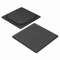
IC TXRX ETHERNET MAP 400-BGA
Manufacturer
Maxim Integrated Products
Type
Transceiverr
Datasheet
1.DS33R41.pdf
(335 pages)
Specifications of DS33R41+
Number Of Drivers/receivers
4/4
Protocol
T1/E1/J1
Voltage - Supply
3.14 V ~ 3.47 V
Mounting Type
Surface Mount
Package / Case
400-BGA
Lead Free Status / RoHS Status
Lead free / RoHS Compliant


COL_DET
RX_CRS/
CRS_DV
RX_ERR
RX_CLK
TX_CLK
RX_DV
RXD[0]
RXD[1]
RXD[2]
RXD[3]
NAME
CST
INT
CS
DS33R41 Inverse-Multiplexing Ethernet Mapper with Quad Integrated T1/E1/J1 Transceivers
H16
E15
N20
N19
K19
H18
H19
K18
K20
PIN
L18
J19
J18
W6
TYPE
OZ
IO
IO
O
I
I
I
I
I
I
Chip Select for Protocol Conversion Device. This pin must be taken
low for read/write operations. When CS is high, the RD/DS and WR
signals are ignored.
Chip Select for the T1/E1/J1 Transceivers. Must be low to read or write
the T1/E1/J1 Transceivers
Interrupt Output. Outputs a logic zero when an unmasked interrupt
event is detected. INT is deasserted when all interrupts have been
acknowledged and serviced. Active low. Inactive state is programmable in
register GL.CR1. This pin is deasserted when all interrupts have been
acknowledged and serviced. Active low. Inactive state is programmable in
register GL.CR1.
Collision Detect (MII). Asserted by the MAC PHY to indicate that a
collision is occurring. In DCE Mode this signal should be connected to
ground. This signal is only valid in half duplex mode, and is ignored in full
duplex mode
Receive Carrier Sense (MII). Should be asserted (high) when data from
the PHY (RXD[3:0) is valid. For each clock pulse 4 bits arrive from the
PHY. Bit 0 is the least significant bit. In DCE mode, connect to V
Carrier Sense/Receive Data Valid (RMII). This signal is asserted (high)
when data is valid from the PHY. For each clock pulse 2 bits arrive from
the PHY. In DCE mode, this signal must be grounded.
Receive Clock (MII). Timing reference for RX_DV, RX_ERR and
RXD[3:0], which are clocked on the rising edge. RX_CLK frequency is
25MHz for 100Mbps operation and 2.5MHz for 10Mbps operation. In DTE
mode, this is a clock input provided by the PHY. In DCE mode, this is an
output derived from REF_CLK providing 2.5MHz (10Mbps operation) or
25MHz (100Mbps operation).
Receive Data 0 through 3 (MII). Four bits of received data, sampled
synchronously with the rising edge of RX_CLK. For every clock cycle, the
PHY transfers 4 bits to the DS33R41. RXD[0] is the least significant bit of
the data. Data is not considered valid when RX_DV is low.
Receive Data 0 through 1 (RMII). Two bits of received data, sampled
synchronously with REF_CLK with 100Mbps Mode. Accepted when
CRS_DV is asserted. When configured for 10Mbps Mode, the data is
sampled once every 10 clock periods.
Receive Data Valid (MII). This active high signal indicates valid data from
the PHY. The data RXD is ignored if RX_DV is not asserted high.
Receive Error (MII). Asserted by the MAC PHY for one or more RX_CLK
periods indicating that an error has occurred. Active High indicates
Receive code group is invalid. If CRS_DV is low, RX_ERR has no effect.
This is synchronous with RX_CLK. In DCE mode, this signal must be
grounded.
Receive Error (RMII). Signal is synchronous to REF_CLK;
Transmit Clock (MII). Timing reference for TX_EN and TXD[3:0]. The
TX_CLK frequency is 25MHz for 100Mbps operation and 2.5MHz for
10Mbps operation.
In DTE mode, this is a clock input provided by the PHY. In DCE mode,
this is an output derived from REF_CLK providing 2.5MHz (10Mbps
operation) or 25MHz (100Mbps operation).
MII/RMII PHY PORT
22 of 335
FUNCTION
DD
.
Related parts for DS33R41+
Image
Part Number
Description
Manufacturer
Datasheet
Request
R

Part Number:
Description:
MAX7528KCWPMaxim Integrated Products [CMOS Dual 8-Bit Buffered Multiplying DACs]
Manufacturer:
Maxim Integrated Products
Datasheet:
Part Number:
Description:
Single +5V, fully integrated, 1.25Gbps laser diode driver.
Manufacturer:
Maxim Integrated Products
Datasheet:
Part Number:
Description:
Single +5V, fully integrated, 155Mbps laser diode driver.
Manufacturer:
Maxim Integrated Products
Datasheet:
Part Number:
Description:
VRD11/VRD10, K8 Rev F 2/3/4-Phase PWM Controllers with Integrated Dual MOSFET Drivers
Manufacturer:
Maxim Integrated Products
Datasheet:
Part Number:
Description:
Highly Integrated Level 2 SMBus Battery Chargers
Manufacturer:
Maxim Integrated Products
Datasheet:
Part Number:
Description:
Current Monitor and Accumulator with Integrated Sense Resistor; ; Temperature Range: -40°C to +85°C
Manufacturer:
Maxim Integrated Products
Part Number:
Description:
TSSOP 14/A�/RS-485 Transceivers with Integrated 100O/120O Termination Resis
Manufacturer:
Maxim Integrated Products
Part Number:
Description:
TSSOP 14/A�/RS-485 Transceivers with Integrated 100O/120O Termination Resis
Manufacturer:
Maxim Integrated Products
Part Number:
Description:
QFN 16/A�/AC-DC and DC-DC Peak-Current-Mode Converters with Integrated Step
Manufacturer:
Maxim Integrated Products
Part Number:
Description:
TDFN/A/65V, 1A, 600KHZ, SYNCHRONOUS STEP-DOWN REGULATOR WITH INTEGRATED SWI
Manufacturer:
Maxim Integrated Products
Part Number:
Description:
Integrated Temperature Controller f
Manufacturer:
Maxim Integrated Products
Part Number:
Description:
SOT23-6/I�/45MHz to 650MHz, Integrated IF VCOs with Differential Output
Manufacturer:
Maxim Integrated Products
Part Number:
Description:
SOT23-6/I�/45MHz to 650MHz, Integrated IF VCOs with Differential Output
Manufacturer:
Maxim Integrated Products
Part Number:
Description:
EVALUATION KIT/2.4GHZ TO 2.5GHZ 802.11G/B RF TRANSCEIVER WITH INTEGRATED PA
Manufacturer:
Maxim Integrated Products
Part Number:
Description:
QFN/E/DUAL PCIE/SATA HIGH SPEED SWITCH WITH INTEGRATED BIAS RESISTOR
Manufacturer:
Maxim Integrated Products
Datasheet: