DS33R41+ Maxim Integrated Products, DS33R41+ Datasheet - Page 23
DS33R41+
Manufacturer Part Number
DS33R41+
Description
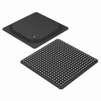
IC TXRX ETHERNET MAP 400-BGA
Manufacturer
Maxim Integrated Products
Type
Transceiverr
Datasheet
1.DS33R41.pdf
(335 pages)
Specifications of DS33R41+
Number Of Drivers/receivers
4/4
Protocol
T1/E1/J1
Voltage - Supply
3.14 V ~ 3.47 V
Mounting Type
Surface Mount
Package / Case
400-BGA
Lead Free Status / RoHS Status
Lead free / RoHS Compliant


REF_CLKO
DCEDTES
REF_CLK
RMIIMIIS
TX_EN
TXD[0]
TXD[1]
TXD[2]
TXD[3]
NAME
SDCS
MDIO
SCAS
SRAS
MDC
DS33R41 Inverse-Multiplexing Ethernet Mapper with Quad Integrated T1/E1/J1 Transceivers
M19
M18
M20
G19
C20
K13
E20
R14
P15
R15
PIN
L20
L19
L17
F20
TYPE
IO
O
O
O
O
O
O
O
I
I
I
Transmit Data 0 through 3(MII). TXD [3:0] is presented synchronously
with the rising edge of TX_CLK. TXD [0] is the least significant bit of the
data. When TX_EN is low the data on TXD should be ignored.
Transmit Data 0 through 1(RMII). Two bits of data TXD [1:0] presented
synchronously with the rising edge of REF_CLK.
Transmit Enable (MII). This pin is asserted high when data TXD [3:0] is
being provided by the DS33R41. The signal is deasserted prior to the first
nibble of the next frame. This signal is synchronous with the rising edge
TX_CLK. It is asserted with the first bit of the preamble.
Transmit Enable (RMII). When this signal is asserted, the data on TXD
[1:0] is valid. This signal is synchronous to the REF_CLK.
Reference Clock (RMII and MII). When in RMII mode, all signals from
the PHY are synchronous to this clock input for both transmit and receive.
This required clock can be up to 50MHz and should have ±100ppm
accuracy.
When in MII mode in DCE operation, the DS33R41 uses this input to
generate the RX_CLK and TX_CLK outputs as required for the Ethernet
PHY interface. When the MII interface is used with DTE operation, this
clock is not required and should be tied low.
In DCE and RMII modes, this input must have a stable clock input before
setting the RST pin high for normal operation.
Reference Clock Output (RMII and MII). A derived clock output up to
50MHz, generated by internal division of the SYSCLKI signal. Frequency
accuracy of the REF_CLKO signal will be proportional to the accuracy of
the user-supplied SYSCLKI signal. See Section
information.
DCE or DTE Selection. The user must set this pin high for DCE Mode
selection or low for DTE Mode. In DCE Mode, the DS33R41 MAC port
can be directly connected to another MAC. In DCE Mode, the Transmit
clock (TX_CLK) and Receive clock (RX_CLK) are output by the
DS33R41. Note that there is no software bit selection of DCEDTES. Note
that DCE Mode is only relevant when the MAC interface is in MII mode.
RMII or MII Selection. Set high to configure the MAC for RMII interfacing.
Set low for MII interfacing.
Management Data Clock (MII). Clocks management data between the
PHY and DS33R41. The clock is derived from the SYSCLKI, with a
maximum frequency is 1.67MHz. The user must leave this pin
unconnected in the DCE Mode.
MII Management data IO (MII). Data path for control information between
the PHY and DS33R41. When not used, pull to logic high externally
through a 10kΩ resistor. The MDC and MDIO pins are used to write or
read up to 32 Control and Status Registers in 32 PHY Controllers. This
port can also be used to initiate Auto-Negotiation for the PHY. The user
must leave this pin unconnected in the DCE Mode.
SDRAM Column Address Strobe. Active low output, used to latch the
column address on the rising edge of SDCLKO. It is used with commands
for Bank Activate, Precharge, and Mode Register Write.
SDRAM Row Address Strobe. Active low output, used to latch the row
address on rising edge of SDCLKO. It is used with commands for Bank
Activate, Precharge, and Mode Register Write.
SDRAM Chip Select. Active low output enables SDRAM access.
PHY MANAGEMENT BUS
SDRAM CONTROLLER
23 of 335
FUNCTION
9.1.2
for more
Related parts for DS33R41+
Image
Part Number
Description
Manufacturer
Datasheet
Request
R

Part Number:
Description:
MAX7528KCWPMaxim Integrated Products [CMOS Dual 8-Bit Buffered Multiplying DACs]
Manufacturer:
Maxim Integrated Products
Datasheet:
Part Number:
Description:
Single +5V, fully integrated, 1.25Gbps laser diode driver.
Manufacturer:
Maxim Integrated Products
Datasheet:
Part Number:
Description:
Single +5V, fully integrated, 155Mbps laser diode driver.
Manufacturer:
Maxim Integrated Products
Datasheet:
Part Number:
Description:
VRD11/VRD10, K8 Rev F 2/3/4-Phase PWM Controllers with Integrated Dual MOSFET Drivers
Manufacturer:
Maxim Integrated Products
Datasheet:
Part Number:
Description:
Highly Integrated Level 2 SMBus Battery Chargers
Manufacturer:
Maxim Integrated Products
Datasheet:
Part Number:
Description:
Current Monitor and Accumulator with Integrated Sense Resistor; ; Temperature Range: -40°C to +85°C
Manufacturer:
Maxim Integrated Products
Part Number:
Description:
TSSOP 14/A�/RS-485 Transceivers with Integrated 100O/120O Termination Resis
Manufacturer:
Maxim Integrated Products
Part Number:
Description:
TSSOP 14/A�/RS-485 Transceivers with Integrated 100O/120O Termination Resis
Manufacturer:
Maxim Integrated Products
Part Number:
Description:
QFN 16/A�/AC-DC and DC-DC Peak-Current-Mode Converters with Integrated Step
Manufacturer:
Maxim Integrated Products
Part Number:
Description:
TDFN/A/65V, 1A, 600KHZ, SYNCHRONOUS STEP-DOWN REGULATOR WITH INTEGRATED SWI
Manufacturer:
Maxim Integrated Products
Part Number:
Description:
Integrated Temperature Controller f
Manufacturer:
Maxim Integrated Products
Part Number:
Description:
SOT23-6/I�/45MHz to 650MHz, Integrated IF VCOs with Differential Output
Manufacturer:
Maxim Integrated Products
Part Number:
Description:
SOT23-6/I�/45MHz to 650MHz, Integrated IF VCOs with Differential Output
Manufacturer:
Maxim Integrated Products
Part Number:
Description:
EVALUATION KIT/2.4GHZ TO 2.5GHZ 802.11G/B RF TRANSCEIVER WITH INTEGRATED PA
Manufacturer:
Maxim Integrated Products
Part Number:
Description:
QFN/E/DUAL PCIE/SATA HIGH SPEED SWITCH WITH INTEGRATED BIAS RESISTOR
Manufacturer:
Maxim Integrated Products
Datasheet: