CY7C68014A-56BAXC Cypress Semiconductor Corp, CY7C68014A-56BAXC Datasheet - Page 58
CY7C68014A-56BAXC
Manufacturer Part Number
CY7C68014A-56BAXC
Description
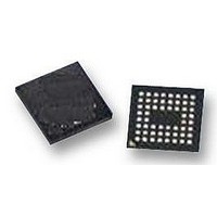
IC MCU USB PERIPH HI SPD 56VFBGA
Manufacturer
Cypress Semiconductor Corp
Series
EZ-USB FX2LP™r
Specifications of CY7C68014A-56BAXC
Applications
USB Microcontroller
Core Processor
8051
Program Memory Type
ROMless
Controller Series
CY7C680xx
Ram Size
16K x 8
Interface
I²C, USB, USART
Number Of I /o
24
Voltage - Supply
3 V ~ 3.6 V
Operating Temperature
0°C ~ 70°C
Mounting Type
Surface Mount
Package / Case
56-VFBGA
Core Size
16bit
No. Of I/o's
24
Program Memory Size
16KB
Ram Memory Size
16KB
Cpu Speed
48MHz
Oscillator Type
External Only
No. Of Timers
3
Digital Ic Case Style
VFBGA
Supply Voltage Range
3V
Controller Family/series
EZ-USB FX2LP
Rohs Compliant
Yes
Lead Free Status / RoHS Status
Lead free / RoHS Compliant
For Use With
CY4611B - KIT USB TO ATA REFERENCE DESIGN
Lead Free Status / RoHS Status
Lead free / RoHS Compliant, Lead free / RoHS Compliant
Available stocks
Company
Part Number
Manufacturer
Quantity
Price
Company:

Part Number:
CY7C68014A-56BAXC
Manufacturer:
Cypress Semiconductor Corp
Quantity:
10 000


Document #: 38-08032 Rev. *K
Package Diagrams
13.0
The following recommendations should be followed to ensure
reliable high-performance operation.
Note:
24. Source for recommendations: EZ-USB FX2™PCB Design Recommendations, http://www.cypress.com/cfuploads/support/app_notes/FX2_PCB.pdf and High
• At least a four-layer impedance controlled boards are re-
• Specify impedance targets (ask your board vendor what
• To control impedance, maintain trace widths and trace spac-
• Minimize stubs to minimize reflected signals.
• Connections between the USB connector shell and signal
• Bypass/flyback caps on VBus, near connector, are recom-
• DPLUS and DMINUS trace lengths should be kept to within
quired to maintain signal quality.
they can achieve).
ing.
ground must be done near the USB connector.
mended.
2 mm of each other in length, with preferred length of
20–30 mm.
Speed USB Platform Design Guidelines, http://www.usb.org/developers/docs/hs_usb_pdg_r1_0.pdf.
PCB Layout Recommendations
PIN A1 CORNER
A
C
G
B
D
E
F
H
-C-
1
SEATING PLANE
2
SIDE VIEW
(continued)
3
5.00±0.10
TOP VIEW
4
Figure 12-5. 56 VFBGA (5 x 5 x 1.0 mm) 0.50 Pitch, 0.30 Ball BZ56
5
6
6
8
[24]
14.0
Package Design Notes
Electrical contact of the part to the Printed Circuit Board (PCB)
is made by soldering the leads on the bottom surface of the
package to the PCB. Hence, special attention is required to the
heat transfer area below the package to provide a good
thermal bond to the circuit board. A Copper (Cu) fill is to be
designed into the PCB as a thermal pad under the package.
Heat is transferred from the FX2LP through the device’s metal
paddle on the bottom side of the package. Heat from here, is
conducted to the PCB at the thermal pad. It is then conducted
• Maintain a solid ground plane under the DPLUS and DMI-
• It is preferred is to have no vias placed on the DPLUS or
• Isolate the DPLUS and DMINUS traces from all other signal
NUS traces. Do not allow the plane to be split under these
traces.
DMINUS trace routing.
traces by no less than 10 mm.
PACKAGE WEIGHT: 0.02 grams
REFERENCE JEDEC: MO-195C
Quad Flat Package No Leads (QFN)
-B-
CY7C68013A/CY7C68014A
CY7C68015A/CY7C68016A
0.10(4X)
-A-
BOTTOM VIEW
8
7
Ø0.05 M C
Ø0.30±0.05(56X)
Ø0.15 M C A B
6
5.00±0.10
5
0.50
3.50
4
001-03901-*B
3
2
1
A1 CORNER
A
C
G
B
D
E
F
H
Page 58 of 60
Related parts for CY7C68014A-56BAXC
Image
Part Number
Description
Manufacturer
Datasheet
Request
R

Part Number:
Description:
IC MCU USB PERIPH HI SPD 56SSOP
Manufacturer:
Cypress Semiconductor Corp
Datasheet:

Part Number:
Description:
IC MCU USB PERIPH HI SPD 100LQFP
Manufacturer:
Cypress Semiconductor Corp
Datasheet:

Part Number:
Description:
IC MCU USB PHERIPH FX2LP 56VQFN
Manufacturer:
Cypress Semiconductor Corp
Datasheet:

Part Number:
Description:
IC MCU USB PERIPH HI SPD 128LQFP
Manufacturer:
Cypress Semiconductor Corp
Datasheet:
Part Number:
Description:
IC MCU USB PERIPH HI SPD 56VQFN
Manufacturer:
Cypress Semiconductor Corp
Datasheet:
Part Number:
Description:
Manufacturer:
Cypress Semiconductor Corp
Datasheet:
Part Number:
Description:
Manufacturer:
Cypress Semiconductor Corp
Datasheet:
Part Number:
Description:
Manufacturer:
Cypress Semiconductor Corp
Datasheet: