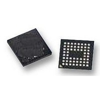
CY7C68014A-56BAXC Cypress Semiconductor Corp, CY7C68014A-56BAXC Datasheet - Page 14

CY7C68014A-56BAXC
Manufacturer Part Number
CY7C68014A-56BAXC
Description
IC MCU USB PERIPH HI SPD 56VFBGA
Manufacturer
Cypress Semiconductor Corp
Series
EZ-USB FX2LP™r
Specifications of CY7C68014A-56BAXC
Applications
USB Microcontroller
Core Processor
8051
Program Memory Type
ROMless
Controller Series
CY7C680xx
Ram Size
16K x 8
Interface
I²C, USB, USART
Number Of I /o
24
Voltage - Supply
3 V ~ 3.6 V
Operating Temperature
0°C ~ 70°C
Mounting Type
Surface Mount
Package / Case
56-VFBGA
Core Size
16bit
No. Of I/o's
24
Program Memory Size
16KB
Ram Memory Size
16KB
Cpu Speed
48MHz
Oscillator Type
External Only
No. Of Timers
3
Digital Ic Case Style
VFBGA
Supply Voltage Range
3V
Controller Family/series
EZ-USB FX2LP
Rohs Compliant
Yes
Lead Free Status / RoHS Status
Lead free / RoHS Compliant
For Use With
CY4611B - KIT USB TO ATA REFERENCE DESIGN
Lead Free Status / RoHS Status
Lead free / RoHS Compliant, Lead free / RoHS Compliant
Available stocks
Company
Part Number
Manufacturer
Quantity
Price
Company:
Part Number:
CY7C68014A-56BAXC
Manufacturer:
Cypress Semiconductor Corp
Quantity:
10 000
Document #: 38-08032 Rev. *K
4.0
Figure 4-1 identifies all signals for the five package types. The
following pages illustrate the individual pin diagrams, plus a
combination diagram showing which of the full set of signals
are available in the 128-, 100-, and 56-pin packages.
The signals on the left edge of the 56-pin package in
Figure 4-1 are common to all versions in the FX2LP family with
the noted differences between the CY7C68013A and the
CY7C68015A. Three modes are available in all package
versions: Port, GPIF master, and Slave FIFO. These modes
define the signals on the right edge of the diagram. The 8051
selects the interface mode using the IFCONFIG[1:0] register
bits. Port mode is the power-on default configuration.
The 100-pin package adds functionality to the 56-pin package
by adding these pins:
• PORTC or alternate GPIFADR[7:0] address signals
Pin Assignments
The 128-pin package adds the 8051 address and data buses
plus control signals. Note that two of the required signals, RD#
and WR#, are present in the 100-pin version. In the 100-pin
and 128-pin versions, an 8051 control bit can be set to pulse
the RD# and WR# pins when the 8051 reads from/writes to
PORTC. This feature is enabled by setting PORTCSTB bit in
CPUCS register.
Section 10.5 displays the timing diagram of the read and write
strobing function on accessing PORTC.
• PORTE or alternate GPIFADR[8] address signal and seven
• Three GPIF Control signals
• Four GPIF Ready signals
• Nine 8051 signals (two USARTs, three timer inputs,
• BKPT, RD#, WR#.
additional 8051 signals
INT4,and INT5#)
CY7C68013A/CY7C68014A
CY7C68015A/CY7C68016A
Page 14 of 60


