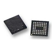
CY7C68014A-56BAXC Cypress Semiconductor Corp, CY7C68014A-56BAXC Datasheet - Page 59

CY7C68014A-56BAXC
Manufacturer Part Number
CY7C68014A-56BAXC
Description
IC MCU USB PERIPH HI SPD 56VFBGA
Manufacturer
Cypress Semiconductor Corp
Series
EZ-USB FX2LP™r
Specifications of CY7C68014A-56BAXC
Applications
USB Microcontroller
Core Processor
8051
Program Memory Type
ROMless
Controller Series
CY7C680xx
Ram Size
16K x 8
Interface
I²C, USB, USART
Number Of I /o
24
Voltage - Supply
3 V ~ 3.6 V
Operating Temperature
0°C ~ 70°C
Mounting Type
Surface Mount
Package / Case
56-VFBGA
Core Size
16bit
No. Of I/o's
24
Program Memory Size
16KB
Ram Memory Size
16KB
Cpu Speed
48MHz
Oscillator Type
External Only
No. Of Timers
3
Digital Ic Case Style
VFBGA
Supply Voltage Range
3V
Controller Family/series
EZ-USB FX2LP
Rohs Compliant
Yes
Lead Free Status / RoHS Status
Lead free / RoHS Compliant
For Use With
CY4611B - KIT USB TO ATA REFERENCE DESIGN
Lead Free Status / RoHS Status
Lead free / RoHS Compliant, Lead free / RoHS Compliant
Available stocks
Company
Part Number
Manufacturer
Quantity
Price
Company:
Part Number:
CY7C68014A-56BAXC
Manufacturer:
Cypress Semiconductor Corp
Quantity:
10 000
from the thermal pad to the PCB inner ground plane by a 5 x 5
array of via. A via is a plated through hole in the PCB with a
finished diameter of 13 mil. The QFN’s metal die paddle must
be soldered to the PCB’s thermal pad. Solder mask is placed
on the board top side over each via to resist solder flow into
the via. The mask on the top side also minimizes outgassing
during the solder reflow process.
For further information on this package design please refer to
the application note Surface Mount Assembly of AMKOR’s
MicroLeadFrame (MLF) Technology. This application note can
be downloaded from AMKOR’s website from the following
URL
http://www.amkor.com/products/notes_papers/MLF_AppNote
_0902.pdf. The application note provides detailed information
on board mounting guidelines, soldering flow, rework process,
etc.
Purchase of I
I
as defined by Philips. EZ-USB FX2LP, EZ-USB FX2 and ReNumeration are trademarks, and EZ-USB is a registered trademark,
of Cypress Semiconductor Corporation. All product and company names mentioned in this document are the trademarks of their
respective holders.
Document #: 38-08032 Rev. *K
© Cypress Semiconductor Corporation, 2006. The information contained herein is subject to change without notice. Cypress Semiconductor Corporation assumes no responsibility for the use
of any circuitry other than circuitry embodied in a Cypress product. Nor does it convey or imply any license under patent or other rights. Cypress products are not warranted nor intended to be
used for medical, life support, life saving, critical control or safety applications, unless pursuant to an express written agreement with Cypress. Furthermore, Cypress does not authorize its
products for use as critical components in life-support systems where a malfunction or failure may reasonably be expected to result in significant injury to the user. The inclusion of Cypress
products in life-support systems application implies that the manufacturer assumes all risk of such use and in doing so indemnifies Cypress against all charges.
2
C Patent Rights to use these components in an I
2
C components from Cypress, or one of its sublicensed Associated Companies, conveys a license under the Philips
Via hole for thermally connecting the
QFN to the circuit board ground plane.
Figure 14-1. Cross-section of the Area Underneath the QFN Package
PCB Material
Figure 14-2. Plot of the Solder Mask (White Area)
Figure 14-3. X-ray Image of the Assembly
Cu Fill
2
C system, provided that the system conforms to the I
Solder Mask
0.013” dia
0.017” dia
Figure 14-1 below displays a cross-sectional area underneath
the package. The cross section is of only one via. The solder
paste template needs to be designed to allow at least 50%
solder coverage. The thickness of the solder paste template
should be 5 mil. It is recommended that “No Clean” type 3
solder paste is used for mounting the part. Nitrogen purge is
recommended during reflow.
Figure 14-2 is a plot of the solder mask pattern and
Figure 14-3 displays an X-Ray image of the assembly (darker
areas indicate solder).
This figure only shows the top three layers of the
circuit board: Top Solder, PCB Dielectric, and
the Ground Plane
Cu Fill
PCB Material
CY7C68013A/CY7C68014A
CY7C68015A/CY7C68016A
2
C Standard Specification
Page 59 of 60


