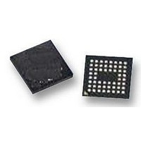
CY7C68014A-56BAXC Cypress Semiconductor Corp, CY7C68014A-56BAXC Datasheet - Page 41

CY7C68014A-56BAXC
Manufacturer Part Number
CY7C68014A-56BAXC
Description
IC MCU USB PERIPH HI SPD 56VFBGA
Manufacturer
Cypress Semiconductor Corp
Series
EZ-USB FX2LP™r
Specifications of CY7C68014A-56BAXC
Applications
USB Microcontroller
Core Processor
8051
Program Memory Type
ROMless
Controller Series
CY7C680xx
Ram Size
16K x 8
Interface
I²C, USB, USART
Number Of I /o
24
Voltage - Supply
3 V ~ 3.6 V
Operating Temperature
0°C ~ 70°C
Mounting Type
Surface Mount
Package / Case
56-VFBGA
Core Size
16bit
No. Of I/o's
24
Program Memory Size
16KB
Ram Memory Size
16KB
Cpu Speed
48MHz
Oscillator Type
External Only
No. Of Timers
3
Digital Ic Case Style
VFBGA
Supply Voltage Range
3V
Controller Family/series
EZ-USB FX2LP
Rohs Compliant
Yes
Lead Free Status / RoHS Status
Lead free / RoHS Compliant
For Use With
CY4611B - KIT USB TO ATA REFERENCE DESIGN
Lead Free Status / RoHS Status
Lead free / RoHS Compliant, Lead free / RoHS Compliant
Available stocks
Company
Part Number
Manufacturer
Quantity
Price
Company:
Part Number:
CY7C68014A-56BAXC
Manufacturer:
Cypress Semiconductor Corp
Quantity:
10 000
Document #: 38-08032 Rev. *K
10.5
The RD# and WR# are present in the 100-pin version and the
128-pin package. In these 100-pin and 128-pin versions, an
8051 control bit can be set to pulse the RD# and WR# pins
when the 8051 reads from/writes to PORTC. This feature is
enabled by setting PORTCSTB bit in CPUCS register.
The RD# and WR# strobes are asserted for two CLKOUT
cycles when PORTC is accessed.
The WR# strobe will be asserted two clock cycles after
PORTC is updated and will be active for two clock cycles after
that as shown in Figure 10-4.
As for read, the value of PORTC three clock cycles before the
assertion of RD# is the value that the 8051 reads in. The RD#
is pulsed for 2 clock cycles after 3 clock cycles from the point
when the 8051 has performed a read function on PORTC.
PORTC IS UPDATED
CLKOUT
WR#
CLKOUT
8051 READS PORTC
RD#
PORTC Strobe Feature Timings
Figure 10-5. RD# Strobe Function when PORTC is Accessed by 8051
Figure 10-4. WR# Strobe Function when PORTC is Accessed by 8051
t
t
CLKOUT
CLKOUT
DATA MUST BE HELD FOR 3 CLK CYLCES
t
The way the feature is intended to work is that the RD# signal
will prompt the external logic to prepare the next data byte.
Nothing gets sampled internally on assertion of the RD# signal
itself. It is just a “prefetch” type signal to get the next data byte
prepared. So, using it with that in mind should easily meet the
set-up time to the next read.
The purpose of this pulsing of RD# is to let the external
peripheral know that the 8051 is done reading PORTC and the
data was latched into PORTC three CLKOUT cycles prior to
asserting the RD# signal. Once the RD# is pulsed the external
logic may update the data on PORTC.
Following is the timing diagram of the read and write strobing
function on accessing PORTC. Refer to Section 10.3 and
Section 10.4 for details on propagation delay of RD# and WR#
signals.
STBL
t
STBL
CY7C68013A/CY7C68014A
CY7C68015A/CY7C68016A
DATA CAN BE UPDATED BY EXTERNAL LOGIC
t
STBH
t
STBH
Page 41 of 60


