CY7C68014A-56BAXC Cypress Semiconductor Corp, CY7C68014A-56BAXC Datasheet - Page 39
CY7C68014A-56BAXC
Manufacturer Part Number
CY7C68014A-56BAXC
Description
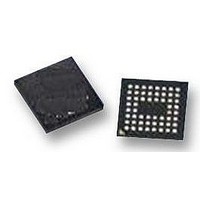
IC MCU USB PERIPH HI SPD 56VFBGA
Manufacturer
Cypress Semiconductor Corp
Series
EZ-USB FX2LP™r
Specifications of CY7C68014A-56BAXC
Applications
USB Microcontroller
Core Processor
8051
Program Memory Type
ROMless
Controller Series
CY7C680xx
Ram Size
16K x 8
Interface
I²C, USB, USART
Number Of I /o
24
Voltage - Supply
3 V ~ 3.6 V
Operating Temperature
0°C ~ 70°C
Mounting Type
Surface Mount
Package / Case
56-VFBGA
Core Size
16bit
No. Of I/o's
24
Program Memory Size
16KB
Ram Memory Size
16KB
Cpu Speed
48MHz
Oscillator Type
External Only
No. Of Timers
3
Digital Ic Case Style
VFBGA
Supply Voltage Range
3V
Controller Family/series
EZ-USB FX2LP
Rohs Compliant
Yes
Lead Free Status / RoHS Status
Lead free / RoHS Compliant
For Use With
CY4611B - KIT USB TO ATA REFERENCE DESIGN
Lead Free Status / RoHS Status
Lead free / RoHS Compliant, Lead free / RoHS Compliant
Available stocks
Company
Part Number
Manufacturer
Quantity
Price
Company:

Part Number:
CY7C68014A-56BAXC
Manufacturer:
Cypress Semiconductor Corp
Quantity:
10 000


Document #: 38-08032 Rev. *K
10.3
Table 10-2. Data Memory Read Parameters
t
t
t
t
t
t
t
t
When using the AUTPOPTR1 or AUTOPTR2 to address external memory, the address of AUTOPTR1 will only be active while
either RD# or WR# are active. The address of AUTOPTR2 will be active throughout the cycle and meet the above address valid
time for which is based on the stretch value
Note:
19. t
CL
AV
STBL
STBH
SCSL
SOEL
DSU
DH
Parameter
t
t
t
t
ACC2
ACC2
ACC2
ACC3
ACC3
CLKOUT
CLKOUT
Data Memory Read
(24 MHz) = 3*t
(48 MHz) = 3*t
(24 MHz) = 5*t
(48 MHz) = 5*t
and t
ACC3
A[15..0]
A[15..0]
[17]
[17]
D[7..0]
D[7..0]
are computed from the above parameters as follows:
1/CLKOUT Frequency
Delay from Clock to Valid Address
Clock to RD LOW
Clock to RD HIGH
Clock to CS LOW
Clock to OE LOW
Data Set-up to Clock
Data Hold Time
RD#
OE#
RD#
CS#
CS#
CL
CL
CL
CL
– t
– t
– t
– t
AV
AV
AV
AV
–t
– t
–t
– t
DSU
DSU
DSU
DSU
t
t
AV
AV
t
t
CL
CL
= 106 ns
= 190 ns
= 43 ns
= 86 ns.
Description
Figure 10-2. Data Memory Read Timing Diagram
t
STBL
t
t
ACC1
SCSL
t
SOEL
[19
Stretch = 0
Stretch = 1
t
data in
DSU
t
ACC1
Min.
[19]
9.6
t
0
STBH
t
DH
20.83
41.66
Typ.
83.2
t
CY7C68013A/CY7C68014A
CY7C68015A/CY7C68016A
AV
t
data in
DSU
Max.
10.7
11.1
11
13
11
t
DH
Unit
ns
ns
ns
ns
ns
ns
ns
ns
ns
ns
Page 39 of 60
48 MHz
24 MHz
12 MHz
Notes
Related parts for CY7C68014A-56BAXC
Image
Part Number
Description
Manufacturer
Datasheet
Request
R

Part Number:
Description:
IC MCU USB PERIPH HI SPD 56SSOP
Manufacturer:
Cypress Semiconductor Corp
Datasheet:

Part Number:
Description:
IC MCU USB PERIPH HI SPD 100LQFP
Manufacturer:
Cypress Semiconductor Corp
Datasheet:

Part Number:
Description:
IC MCU USB PHERIPH FX2LP 56VQFN
Manufacturer:
Cypress Semiconductor Corp
Datasheet:

Part Number:
Description:
IC MCU USB PERIPH HI SPD 128LQFP
Manufacturer:
Cypress Semiconductor Corp
Datasheet:
Part Number:
Description:
IC MCU USB PERIPH HI SPD 56VQFN
Manufacturer:
Cypress Semiconductor Corp
Datasheet:
Part Number:
Description:
Manufacturer:
Cypress Semiconductor Corp
Datasheet:
Part Number:
Description:
Manufacturer:
Cypress Semiconductor Corp
Datasheet:
Part Number:
Description:
Manufacturer:
Cypress Semiconductor Corp
Datasheet: