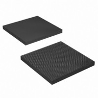
EP4SGX290KF40C3N Altera, EP4SGX290KF40C3N Datasheet - Page 689

EP4SGX290KF40C3N
Manufacturer Part Number
EP4SGX290KF40C3N
Description
IC STRATIX IV GX 290K 1517FBGA
Manufacturer
Altera
Series
Stratix® IV GXr
Datasheets
1.EP4SGX110DF29C3N.pdf
(80 pages)
2.EP4SGX110DF29C3N.pdf
(1154 pages)
3.EP4SGX110DF29C3N.pdf
(432 pages)
4.EP4SGX110DF29C3N.pdf
(22 pages)
5.EP4SGX110DF29C3N.pdf
(30 pages)
6.EP4SGX110DF29C3N.pdf
(72 pages)
Specifications of EP4SGX290KF40C3N
Number Of Logic Elements/cells
291200
Number Of Labs/clbs
11648
Total Ram Bits
17248
Number Of I /o
744
Voltage - Supply
0.87 V ~ 0.93 V
Mounting Type
Surface Mount
Operating Temperature
0°C ~ 85°C
Package / Case
1517-FBGA
Lead Free Status / RoHS Status
Lead free / RoHS Compliant
Number Of Gates
-
Other names
544-2624
Available stocks
Company
Part Number
Manufacturer
Quantity
Price
- EP4SGX110DF29C3N PDF datasheet
- EP4SGX110DF29C3N PDF datasheet #2
- EP4SGX110DF29C3N PDF datasheet #3
- EP4SGX110DF29C3N PDF datasheet #4
- EP4SGX110DF29C3N PDF datasheet #5
- EP4SGX110DF29C3N PDF datasheet #6
- Current page: 689 of 1154
- Download datasheet (32Mb)
Chapter 2: Transceiver Clocking in Stratix IV Devices
FPGA Fabric PLLs-Transceiver PLLs Cascading
Figure 2–11. Left and Right, Left, or Right PLL in VCO Bypass Mode
February 2011 Altera Corporation
from the dedicated
Reference clock
CLK pin
Left and Right, Left, or Right PLL in VCO Bypass Mode
f
If all CMU channels on the same side of the device are configured as channels, all
refclk pins are used as receiver serial input data pins. All CMU PLLs are also used as
receiver CDRs. In such designs, you must use the 6G ATX PLLs to generate the
high-speed serial and low-speed parallel transceiver clocks provided that the
configured data rate is supported by the 6G ATX PLLs. Additionally, Altera
recommends providing the input reference clock to the 6G ATX PLL using the left or
right PLL cascade clock line because none of the refclk pins are available. To avoid
jitter amplification because of cascading of the left or right PLL to the 6G ATX PLL,
you must place the left or right PLL in VCO bypass mode.
For more information about CMU PLLs, refer to “Configuring CMU Channels as
Transceiver Channels” in the
Figure 2–11
dedicated FPGA CLK pins to the inclk port of the left and right, left, or right PLL
bypasses the PLL loop and is driven directly on the PLL output clock port.
/N
shows that in VCO bypass mode, the input reference clock from the
Frequency
Detector
Phase
Transceiver Architecture in Stratix IV Devices
Charge Pump
Left and Right PLL
Loop Filter
+
/M
Controlled
Oscillator
Voltage
Stratix IV Device Handbook Volume 2: Transceivers
C1
chapter.
Input reference
6G ATX PLL
clock to the
2–17
Related parts for EP4SGX290KF40C3N
Image
Part Number
Description
Manufacturer
Datasheet
Request
R

Part Number:
Description:
CYCLONE II STARTER KIT EP2C20N
Manufacturer:
Altera
Datasheet:

Part Number:
Description:
CPLD, EP610 Family, ECMOS Process, 300 Gates, 16 Macro Cells, 16 Reg., 16 User I/Os, 5V Supply, 35 Speed Grade, 24DIP
Manufacturer:
Altera Corporation
Datasheet:

Part Number:
Description:
CPLD, EP610 Family, ECMOS Process, 300 Gates, 16 Macro Cells, 16 Reg., 16 User I/Os, 5V Supply, 15 Speed Grade, 24DIP
Manufacturer:
Altera Corporation
Datasheet:

Part Number:
Description:
Manufacturer:
Altera Corporation
Datasheet:

Part Number:
Description:
CPLD, EP610 Family, ECMOS Process, 300 Gates, 16 Macro Cells, 16 Reg., 16 User I/Os, 5V Supply, 30 Speed Grade, 24DIP
Manufacturer:
Altera Corporation
Datasheet:

Part Number:
Description:
High-performance, low-power erasable programmable logic devices with 8 macrocells, 10ns
Manufacturer:
Altera Corporation
Datasheet:

Part Number:
Description:
High-performance, low-power erasable programmable logic devices with 8 macrocells, 7ns
Manufacturer:
Altera Corporation
Datasheet:

Part Number:
Description:
Classic EPLD
Manufacturer:
Altera Corporation
Datasheet:

Part Number:
Description:
High-performance, low-power erasable programmable logic devices with 8 macrocells, 10ns
Manufacturer:
Altera Corporation
Datasheet:

Part Number:
Description:
Manufacturer:
Altera Corporation
Datasheet:

Part Number:
Description:
Manufacturer:
Altera Corporation
Datasheet:

Part Number:
Description:
Manufacturer:
Altera Corporation
Datasheet:

Part Number:
Description:
CPLD, EP610 Family, ECMOS Process, 300 Gates, 16 Macro Cells, 16 Reg., 16 User I/Os, 5V Supply, 25 Speed Grade, 24DIP
Manufacturer:
Altera Corporation
Datasheet:


