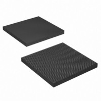
EP4SGX290KF40C3N Altera, EP4SGX290KF40C3N Datasheet - Page 282

EP4SGX290KF40C3N
Manufacturer Part Number
EP4SGX290KF40C3N
Description
IC STRATIX IV GX 290K 1517FBGA
Manufacturer
Altera
Series
Stratix® IV GXr
Datasheets
1.EP4SGX110DF29C3N.pdf
(80 pages)
2.EP4SGX110DF29C3N.pdf
(1154 pages)
3.EP4SGX110DF29C3N.pdf
(432 pages)
4.EP4SGX110DF29C3N.pdf
(22 pages)
5.EP4SGX110DF29C3N.pdf
(30 pages)
6.EP4SGX110DF29C3N.pdf
(72 pages)
Specifications of EP4SGX290KF40C3N
Number Of Logic Elements/cells
291200
Number Of Labs/clbs
11648
Total Ram Bits
17248
Number Of I /o
744
Voltage - Supply
0.87 V ~ 0.93 V
Mounting Type
Surface Mount
Operating Temperature
0°C ~ 85°C
Package / Case
1517-FBGA
Lead Free Status / RoHS Status
Lead free / RoHS Compliant
Number Of Gates
-
Other names
544-2624
Available stocks
Company
Part Number
Manufacturer
Quantity
Price
- EP4SGX110DF29C3N PDF datasheet
- EP4SGX110DF29C3N PDF datasheet #2
- EP4SGX110DF29C3N PDF datasheet #3
- EP4SGX110DF29C3N PDF datasheet #4
- EP4SGX110DF29C3N PDF datasheet #5
- EP4SGX110DF29C3N PDF datasheet #6
- Current page: 282 of 1154
- Download datasheet (32Mb)
8–4
Figure 8–3. High-Speed Differential I/Os with DPA Locations in Stratix IV GT and GX Devices
LVDS Channels
Stratix IV Device Handbook Volume 1
1
Figure 8–3
The Stratix IV device family supports LVDS on both row and column I/O banks. Row
I/Os support true LVDS input with 100-Ω differential input termination (OCT R
and true LVDS output buffers. Column I/Os supports true LVDS input buffers
without OCT R
emulated LVDS output buffers that use two single-ended output buffers with an
external resistor network to support LVDS, mini-LVDS, and RSDS standards.
Stratix IV devices offer single-ended I/O refclk support for the LVDS.
Dedicated SERDES and DPA circuitries are implemented on the row I/O banks to
further enhance LVDS interface performance in the device. For column I/O banks,
SERDES is implemented in the core logic because there is no dedicated SERDES
circuitry on column I/O banks.
Emulated differential output buffers support tri-state capability starting with the
Quartus II software version 9.1.
shows a high-level chip overview of the Stratix IV GT and GX devices.
General Purpose
General Purpose
I/O and Memory
I/O and Memory
PLL
PLL
PLL
PLL
D
Interface
Interface
. Alternately, you can configure the row and column LVDS pins as
(Logic Elements, DSP,
Embedded Memory,
Chapter 8: High-Speed Differential I/O Interfaces and DPA in Stratix IV Devices
Clock Networks)
FPGA Fabric
PLL
PLL
PLL
PLL
General Purpose
General Purpose
I/O and Memory
I/O and Memory
Interface
Interface
PLL
PLL
PLL
PLL
February 2011 Altera Corporation
LVDS Channels
D
),
Related parts for EP4SGX290KF40C3N
Image
Part Number
Description
Manufacturer
Datasheet
Request
R

Part Number:
Description:
CYCLONE II STARTER KIT EP2C20N
Manufacturer:
Altera
Datasheet:

Part Number:
Description:
CPLD, EP610 Family, ECMOS Process, 300 Gates, 16 Macro Cells, 16 Reg., 16 User I/Os, 5V Supply, 35 Speed Grade, 24DIP
Manufacturer:
Altera Corporation
Datasheet:

Part Number:
Description:
CPLD, EP610 Family, ECMOS Process, 300 Gates, 16 Macro Cells, 16 Reg., 16 User I/Os, 5V Supply, 15 Speed Grade, 24DIP
Manufacturer:
Altera Corporation
Datasheet:

Part Number:
Description:
Manufacturer:
Altera Corporation
Datasheet:

Part Number:
Description:
CPLD, EP610 Family, ECMOS Process, 300 Gates, 16 Macro Cells, 16 Reg., 16 User I/Os, 5V Supply, 30 Speed Grade, 24DIP
Manufacturer:
Altera Corporation
Datasheet:

Part Number:
Description:
High-performance, low-power erasable programmable logic devices with 8 macrocells, 10ns
Manufacturer:
Altera Corporation
Datasheet:

Part Number:
Description:
High-performance, low-power erasable programmable logic devices with 8 macrocells, 7ns
Manufacturer:
Altera Corporation
Datasheet:

Part Number:
Description:
Classic EPLD
Manufacturer:
Altera Corporation
Datasheet:

Part Number:
Description:
High-performance, low-power erasable programmable logic devices with 8 macrocells, 10ns
Manufacturer:
Altera Corporation
Datasheet:

Part Number:
Description:
Manufacturer:
Altera Corporation
Datasheet:

Part Number:
Description:
Manufacturer:
Altera Corporation
Datasheet:

Part Number:
Description:
Manufacturer:
Altera Corporation
Datasheet:

Part Number:
Description:
CPLD, EP610 Family, ECMOS Process, 300 Gates, 16 Macro Cells, 16 Reg., 16 User I/Os, 5V Supply, 25 Speed Grade, 24DIP
Manufacturer:
Altera Corporation
Datasheet:


