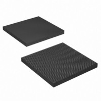
EP4SGX290KF40C3N Altera, EP4SGX290KF40C3N Datasheet - Page 686

EP4SGX290KF40C3N
Manufacturer Part Number
EP4SGX290KF40C3N
Description
IC STRATIX IV GX 290K 1517FBGA
Manufacturer
Altera
Series
Stratix® IV GXr
Datasheets
1.EP4SGX110DF29C3N.pdf
(80 pages)
2.EP4SGX110DF29C3N.pdf
(1154 pages)
3.EP4SGX110DF29C3N.pdf
(432 pages)
4.EP4SGX110DF29C3N.pdf
(22 pages)
5.EP4SGX110DF29C3N.pdf
(30 pages)
6.EP4SGX110DF29C3N.pdf
(72 pages)
Specifications of EP4SGX290KF40C3N
Number Of Logic Elements/cells
291200
Number Of Labs/clbs
11648
Total Ram Bits
17248
Number Of I /o
744
Voltage - Supply
0.87 V ~ 0.93 V
Mounting Type
Surface Mount
Operating Temperature
0°C ~ 85°C
Package / Case
1517-FBGA
Lead Free Status / RoHS Status
Lead free / RoHS Compliant
Number Of Gates
-
Other names
544-2624
Available stocks
Company
Part Number
Manufacturer
Quantity
Price
- EP4SGX110DF29C3N PDF datasheet
- EP4SGX110DF29C3N PDF datasheet #2
- EP4SGX110DF29C3N PDF datasheet #3
- EP4SGX110DF29C3N PDF datasheet #4
- EP4SGX110DF29C3N PDF datasheet #5
- EP4SGX110DF29C3N PDF datasheet #6
- Current page: 686 of 1154
- Download datasheet (32Mb)
2–14
Stratix IV Device Handbook Volume 2: Transceivers
FPGA Fabric PLLs-Transceiver PLLs Cascading Rules
1
You can only cascade the left PLLs (PLL_L1, PLL_L2, PLL_L3, and PLL_L4) to the
transceiver blocks located on the left side of the device. Similarly, you can only
cascade the right PLLs (PLL_R1, PLL_R2, PLL_R3, and PLL_R4) to the transceiver blocks
located on the right side of the device.
The PLL cascade networks are single clock lines segmented by bidirectional tri-state
buffers located along the clock line. Segmentation of the PLL cascade network allows
two left and right PLLs to drive the cascade clock line simultaneously and provides
the input reference clock to the CMU PLLs and receiver CDRs in different transceiver
blocks. When cascading two or more FPGA fabric PLLs to the CMU PLLs and receiver
CDRs, there must be no crossover in the cascaded clock paths on the PLL cascade
network
For better noise rejection, ensure the bandwidth setting of the FPGA fabric PLL (the
upstream PLL) is lower than the transceiver PLL (the downstream PLL).
Example 2: Design Target—EP4SGX530NF45 Device
If your design is targeted for a EP4SGX530NF45 device, it requires providing input
reference clocks to the following CMU PLLs and receiver CDRs from two right PLLs
in the FPGA fabric:
■
■
Case 1: use PLL_R4 to provide the input reference clock to the receiver CDRs in
channel 2 and channel 3 (shown in GREEN) and use PLL_R1 to provide the input
reference clock to the CMU0 PLL (shown in BLUE) in transceiver block GXBR1.
CMU0 PLL in Transceiver Block GXBR1
Receiver CDRs in channel 2 and channel 3 in Transceiver Block GXBR1
(Figure
2–9).
Chapter 2: Transceiver Clocking in Stratix IV Devices
FPGA Fabric PLLs-Transceiver PLLs Cascading
February 2011 Altera Corporation
Related parts for EP4SGX290KF40C3N
Image
Part Number
Description
Manufacturer
Datasheet
Request
R

Part Number:
Description:
CYCLONE II STARTER KIT EP2C20N
Manufacturer:
Altera
Datasheet:

Part Number:
Description:
CPLD, EP610 Family, ECMOS Process, 300 Gates, 16 Macro Cells, 16 Reg., 16 User I/Os, 5V Supply, 35 Speed Grade, 24DIP
Manufacturer:
Altera Corporation
Datasheet:

Part Number:
Description:
CPLD, EP610 Family, ECMOS Process, 300 Gates, 16 Macro Cells, 16 Reg., 16 User I/Os, 5V Supply, 15 Speed Grade, 24DIP
Manufacturer:
Altera Corporation
Datasheet:

Part Number:
Description:
Manufacturer:
Altera Corporation
Datasheet:

Part Number:
Description:
CPLD, EP610 Family, ECMOS Process, 300 Gates, 16 Macro Cells, 16 Reg., 16 User I/Os, 5V Supply, 30 Speed Grade, 24DIP
Manufacturer:
Altera Corporation
Datasheet:

Part Number:
Description:
High-performance, low-power erasable programmable logic devices with 8 macrocells, 10ns
Manufacturer:
Altera Corporation
Datasheet:

Part Number:
Description:
High-performance, low-power erasable programmable logic devices with 8 macrocells, 7ns
Manufacturer:
Altera Corporation
Datasheet:

Part Number:
Description:
Classic EPLD
Manufacturer:
Altera Corporation
Datasheet:

Part Number:
Description:
High-performance, low-power erasable programmable logic devices with 8 macrocells, 10ns
Manufacturer:
Altera Corporation
Datasheet:

Part Number:
Description:
Manufacturer:
Altera Corporation
Datasheet:

Part Number:
Description:
Manufacturer:
Altera Corporation
Datasheet:

Part Number:
Description:
Manufacturer:
Altera Corporation
Datasheet:

Part Number:
Description:
CPLD, EP610 Family, ECMOS Process, 300 Gates, 16 Macro Cells, 16 Reg., 16 User I/Os, 5V Supply, 25 Speed Grade, 24DIP
Manufacturer:
Altera Corporation
Datasheet:


