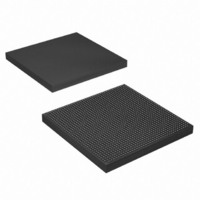
EP4SGX290KF40C3N Altera, EP4SGX290KF40C3N Datasheet - Page 531

EP4SGX290KF40C3N
Manufacturer Part Number
EP4SGX290KF40C3N
Description
IC STRATIX IV GX 290K 1517FBGA
Manufacturer
Altera
Series
Stratix® IV GXr
Datasheets
1.EP4SGX110DF29C3N.pdf
(80 pages)
2.EP4SGX110DF29C3N.pdf
(1154 pages)
3.EP4SGX110DF29C3N.pdf
(432 pages)
4.EP4SGX110DF29C3N.pdf
(22 pages)
5.EP4SGX110DF29C3N.pdf
(30 pages)
6.EP4SGX110DF29C3N.pdf
(72 pages)
Specifications of EP4SGX290KF40C3N
Number Of Logic Elements/cells
291200
Number Of Labs/clbs
11648
Total Ram Bits
17248
Number Of I /o
744
Voltage - Supply
0.87 V ~ 0.93 V
Mounting Type
Surface Mount
Operating Temperature
0°C ~ 85°C
Package / Case
1517-FBGA
Lead Free Status / RoHS Status
Lead free / RoHS Compliant
Number Of Gates
-
Other names
544-2624
Available stocks
Company
Part Number
Manufacturer
Quantity
Price
- EP4SGX110DF29C3N PDF datasheet
- EP4SGX110DF29C3N PDF datasheet #2
- EP4SGX110DF29C3N PDF datasheet #3
- EP4SGX110DF29C3N PDF datasheet #4
- EP4SGX110DF29C3N PDF datasheet #5
- EP4SGX110DF29C3N PDF datasheet #6
- Current page: 531 of 1154
- Download datasheet (32Mb)
Chapter 1: Transceiver Architecture in Stratix IV Devices
Transceiver Block Architecture
Figure 1–72. Rate Match Deletion in Basic Double-Width Mode
Figure 1–73. Rate Match Insertion in Basic Double-Width Mode
February 2011 Altera Corporation
rx_rmfifodatainserted
rx_rmfifodatadeleted
dataout[19:0]
datain[19:10]
dataout[9:0]
datain[9:0]
datain[19:10]
dataout[19:0]
dataout[9:0]
datain[9:0]
The rate match FIFO cannot delete the two skip patterns in this skip cluster because
they do not appear in the same clock cycle. The second skip cluster has a /K28.5/
control pattern in the MSByte of a clock cycle followed by two pairs of /K28.0/ skip
patterns in the next two cycles. The rate match FIFO deletes both pairs of /K28.0/
skip patterns (for a total of four skip patterns deleted) from the second skip cluster to
meet the three skip pattern deletion requirement.
Figure 1–73
skip patterns are required to be inserted. In this example, /K28.5/ is the control
pattern and neutral disparity /K28.0/ is the skip pattern. The first skip cluster has a
/K28.5/ control pattern in the LSByte and /K28.0/ skip pattern in the MSByte of a
clock cycle followed by one /K28.0/ skip pattern in the LSByte of the next clock cycle.
The rate match FIFO inserts pairs of skip patterns in this skip cluster to meet the three
skip pattern insertion requirement.
Dx.y
Dx.y
Dx.y
Dx.y
Dx.y
Dx.y
Dx.y
Dx.y
shows an example of rate match FIFO insertion in the case where three
K28.0
K28.5
K28.0
K28.5
First Skip Cluster
K28.0
K28.5
K28.5
K28.0
First Skip Cluster
Dx.y
Dx.y
K28.0
K28.0
K28.0
K28.0
Dx.y
Dx.y
K28.5
Dx.y
K28.0
K28.0
K28.5
K28.5
Dx.y
Second Skip Cluster
Dx.y
Second Skip Cluster
K28.0
K28.0
Dx.y
Dx.y
Two Pairs of Skip Patterns
K28.0
K28.0
Dx.y
Dx.y
Stratix IV Device Handbook Volume 2: Transceivers
Deleted
K28.0
K28.0
K28.5
Dx.y
K28.0
K28.0
K28.0
K28.0
Dx.y
Dx.y
K28.0
K28.0
1–87
Related parts for EP4SGX290KF40C3N
Image
Part Number
Description
Manufacturer
Datasheet
Request
R

Part Number:
Description:
CYCLONE II STARTER KIT EP2C20N
Manufacturer:
Altera
Datasheet:

Part Number:
Description:
CPLD, EP610 Family, ECMOS Process, 300 Gates, 16 Macro Cells, 16 Reg., 16 User I/Os, 5V Supply, 35 Speed Grade, 24DIP
Manufacturer:
Altera Corporation
Datasheet:

Part Number:
Description:
CPLD, EP610 Family, ECMOS Process, 300 Gates, 16 Macro Cells, 16 Reg., 16 User I/Os, 5V Supply, 15 Speed Grade, 24DIP
Manufacturer:
Altera Corporation
Datasheet:

Part Number:
Description:
Manufacturer:
Altera Corporation
Datasheet:

Part Number:
Description:
CPLD, EP610 Family, ECMOS Process, 300 Gates, 16 Macro Cells, 16 Reg., 16 User I/Os, 5V Supply, 30 Speed Grade, 24DIP
Manufacturer:
Altera Corporation
Datasheet:

Part Number:
Description:
High-performance, low-power erasable programmable logic devices with 8 macrocells, 10ns
Manufacturer:
Altera Corporation
Datasheet:

Part Number:
Description:
High-performance, low-power erasable programmable logic devices with 8 macrocells, 7ns
Manufacturer:
Altera Corporation
Datasheet:

Part Number:
Description:
Classic EPLD
Manufacturer:
Altera Corporation
Datasheet:

Part Number:
Description:
High-performance, low-power erasable programmable logic devices with 8 macrocells, 10ns
Manufacturer:
Altera Corporation
Datasheet:

Part Number:
Description:
Manufacturer:
Altera Corporation
Datasheet:

Part Number:
Description:
Manufacturer:
Altera Corporation
Datasheet:

Part Number:
Description:
Manufacturer:
Altera Corporation
Datasheet:

Part Number:
Description:
CPLD, EP610 Family, ECMOS Process, 300 Gates, 16 Macro Cells, 16 Reg., 16 User I/Os, 5V Supply, 25 Speed Grade, 24DIP
Manufacturer:
Altera Corporation
Datasheet:


