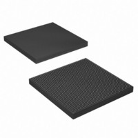
EP4SGX290KF40C3N Altera, EP4SGX290KF40C3N Datasheet - Page 1033

EP4SGX290KF40C3N
Manufacturer Part Number
EP4SGX290KF40C3N
Description
IC STRATIX IV GX 290K 1517FBGA
Manufacturer
Altera
Series
Stratix® IV GXr
Datasheets
1.EP4SGX110DF29C3N.pdf
(80 pages)
2.EP4SGX110DF29C3N.pdf
(1154 pages)
3.EP4SGX110DF29C3N.pdf
(432 pages)
4.EP4SGX110DF29C3N.pdf
(22 pages)
5.EP4SGX110DF29C3N.pdf
(30 pages)
6.EP4SGX110DF29C3N.pdf
(72 pages)
Specifications of EP4SGX290KF40C3N
Number Of Logic Elements/cells
291200
Number Of Labs/clbs
11648
Total Ram Bits
17248
Number Of I /o
744
Voltage - Supply
0.87 V ~ 0.93 V
Mounting Type
Surface Mount
Operating Temperature
0°C ~ 85°C
Package / Case
1517-FBGA
Lead Free Status / RoHS Status
Lead free / RoHS Compliant
Number Of Gates
-
Other names
544-2624
Available stocks
Company
Part Number
Manufacturer
Quantity
Price
- EP4SGX110DF29C3N PDF datasheet
- EP4SGX110DF29C3N PDF datasheet #2
- EP4SGX110DF29C3N PDF datasheet #3
- EP4SGX110DF29C3N PDF datasheet #4
- EP4SGX110DF29C3N PDF datasheet #5
- EP4SGX110DF29C3N PDF datasheet #6
- Current page: 1033 of 1154
- Download datasheet (32Mb)
Chapter 2: Transceiver Design Flow Guide for Stratix IV Devices
Guidelines to Debug Transceiver-Based Designs
February 2011 Altera Corporation
Guidelines to Debug the FPGA Logic and the Transceiver Interface
Before checking the functionality in silicon, perform functional simulation to ensure
the basic functionality of the RTL and the transceiver-FPGA fabric interface.
■
■
■
■
■
■
■
Understand the limitations of functional simulation. If you intend to simulate
timing parameters, consider post-fit simulation. The functional simulation model
for transceivers does not model timing-related parameters or uncertainties in the
transceiver data path. For example, the PPM difference in the rate matcher clocks
(clock rate compensation) or the phase differences between the read and write side
of the phase compensation FIFO are not modeled.
f
Check whether the compiled design has timing violations in the TimeQuest
Timing Analyzer report. Set the appropriate timing constraints on the failing
paths.
f
Verify the functionality of the transmitter and receiver data path with serial
loopback. Dynamically control the serial loopback through the rx_seriallpbken
port. When this signal is asserted, data from the transmitter serializer is looped
back to the receiver CDR of the channel.
Use SignalTap to verify the behavior of the user logic and the transceiver interface
signals. If you have FPGA I/O pins available for debug, you can also use the
external logic analyzer to debug the functionality of the device.
f
1
Verify the interconnect on the receive side by configuring the transceiver in reverse
serial loopback mode. In this case, the recovered data from the receiver channel is
sent to the transmitter buffer. To configure a transceiver channel operating in a
different configuration to reverse serial loopback mode, use the dynamic
reconfiguration controller.
Check whether the transceiver FPGA fabric interface clocking schemes follow the
recommendations provided in the “FPGA Fabric-Transceiver Interface Clocking”
section in the
Ensure that you have used the recommended transceiver reset sequence.
For information about functional RTL simulation or post-fit simulation,
refer to the
For information about using the TimeQuest Timing Analyzer, refer to the
The Quartus II TimeQuest Timing Analyzer
Quartus II Handbook.
For more information, refer to the
Analyzers
To use these features, you must connect the JTAG configuration pins in the
FPGA.
Transceiver Clocking in Stratix IV Devices
chapter in volume 3 of the Quartus II Handbook.
Simulation
chapter in volume 3 of the Quartus II Handbook.
In-System Debugging Using External Logic
chapter in volume 3 of the
chapter.
Stratix IV Device Handbook Volume 3
2–15
Related parts for EP4SGX290KF40C3N
Image
Part Number
Description
Manufacturer
Datasheet
Request
R

Part Number:
Description:
CYCLONE II STARTER KIT EP2C20N
Manufacturer:
Altera
Datasheet:

Part Number:
Description:
CPLD, EP610 Family, ECMOS Process, 300 Gates, 16 Macro Cells, 16 Reg., 16 User I/Os, 5V Supply, 35 Speed Grade, 24DIP
Manufacturer:
Altera Corporation
Datasheet:

Part Number:
Description:
CPLD, EP610 Family, ECMOS Process, 300 Gates, 16 Macro Cells, 16 Reg., 16 User I/Os, 5V Supply, 15 Speed Grade, 24DIP
Manufacturer:
Altera Corporation
Datasheet:

Part Number:
Description:
Manufacturer:
Altera Corporation
Datasheet:

Part Number:
Description:
CPLD, EP610 Family, ECMOS Process, 300 Gates, 16 Macro Cells, 16 Reg., 16 User I/Os, 5V Supply, 30 Speed Grade, 24DIP
Manufacturer:
Altera Corporation
Datasheet:

Part Number:
Description:
High-performance, low-power erasable programmable logic devices with 8 macrocells, 10ns
Manufacturer:
Altera Corporation
Datasheet:

Part Number:
Description:
High-performance, low-power erasable programmable logic devices with 8 macrocells, 7ns
Manufacturer:
Altera Corporation
Datasheet:

Part Number:
Description:
Classic EPLD
Manufacturer:
Altera Corporation
Datasheet:

Part Number:
Description:
High-performance, low-power erasable programmable logic devices with 8 macrocells, 10ns
Manufacturer:
Altera Corporation
Datasheet:

Part Number:
Description:
Manufacturer:
Altera Corporation
Datasheet:

Part Number:
Description:
Manufacturer:
Altera Corporation
Datasheet:

Part Number:
Description:
Manufacturer:
Altera Corporation
Datasheet:

Part Number:
Description:
CPLD, EP610 Family, ECMOS Process, 300 Gates, 16 Macro Cells, 16 Reg., 16 User I/Os, 5V Supply, 25 Speed Grade, 24DIP
Manufacturer:
Altera Corporation
Datasheet:


