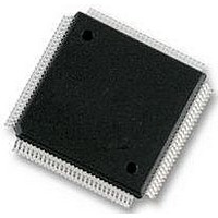
XC68HC12A0CPV8 Freescale Semiconductor, XC68HC12A0CPV8 Datasheet - Page 91

XC68HC12A0CPV8
Manufacturer Part Number
XC68HC12A0CPV8
Description
IC, 16BIT MCU, 68HC12, 8MHZ, TQFP-112
Manufacturer
Freescale Semiconductor
Datasheet
1.MC912D60ACFUE8.pdf
(460 pages)
Specifications of XC68HC12A0CPV8
Controller Family/series
68HC12
No. Of I/o's
68
Eeprom Memory Size
1KB
Ram Memory Size
2KB
Cpu Speed
8MHz
No. Of Timers
1
Core Size
16 Bit
Program Memory Size
60KB
Peripherals
ADC
Lead Free Status / RoHS Status
Lead free / RoHS Compliant
- Current page: 91 of 460
- Download datasheet (5Mb)
MC68HC912D60A — Rev. 3.1
Freescale Semiconductor
In normal expanded modes, the reset vector is located in external
memory. The DBE and ECLK are required for de-multiplexing address
and data, but LSTRB and R/W are only needed by the system when
there are external writable resources. Therefore in normal expanded
modes, only the DBE and ECLK are configured for their alternate bus
control functions and the other bits of port E are configured for general-
purpose I/O. If the normal expanded system needs any other bus-control
signals, PEAR would need to be written before any access that needed
the additional signals.
In special expanded modes, DBE, IPIPE1, IPIPE0, E, LSTRB, and R/W
are configured as bus-control signals.
In peripheral mode, the PEAR register is not accessible for reads or
writes. However, the CGMTE control bit is reset to one to configure PE6
as a test output from the PLL module.
NDBE — No Data Bus Enable
CGMTE — Clock Generator Module Testing Enable
Normal: write once; Special: write anytime EXCEPT the first. Read
anytime.
NDBE controls the use of the DBE pin of Port E. The NDBE bit has no
effect in Single Chip or Peripheral Modes. The associated pin will
default to the CAL function if the CALE bit is set in PEAR register or
otherwise to an I/O.
Normal: write never; Special: write anytime EXCEPT the first. Read
anytime.
0 = PE7 is used for DBE, external control of data enable on
1 = PE7 is the CAL function if CALE bit is set in PEAR register or
0 = PE6 is general-purpose I/O or pipe output.
1 = PE6 is a test signal output from the CGM module (no effect in
memories, or inverted ECLK.
general-purpose I/O.
single chip or normal expanded modes). PIPOE = 1 overrides
this function and forces PE6 to be a pipe status output signal.
Bus Control and Input/Output
Bus Control and Input/Output
Technical Data
Registers
91
Related parts for XC68HC12A0CPV8
Image
Part Number
Description
Manufacturer
Datasheet
Request
R
Part Number:
Description:
Manufacturer:
Freescale Semiconductor, Inc
Datasheet:
Part Number:
Description:
Manufacturer:
Freescale Semiconductor, Inc
Datasheet:
Part Number:
Description:
Manufacturer:
Freescale Semiconductor, Inc
Datasheet:
Part Number:
Description:
Manufacturer:
Freescale Semiconductor, Inc
Datasheet:
Part Number:
Description:
Manufacturer:
Freescale Semiconductor, Inc
Datasheet:
Part Number:
Description:
Manufacturer:
Freescale Semiconductor, Inc
Datasheet:
Part Number:
Description:
Manufacturer:
Freescale Semiconductor, Inc
Datasheet:
Part Number:
Description:
Manufacturer:
Freescale Semiconductor, Inc
Datasheet:
Part Number:
Description:
Manufacturer:
Freescale Semiconductor, Inc
Datasheet:
Part Number:
Description:
Manufacturer:
Freescale Semiconductor, Inc
Datasheet:
Part Number:
Description:
Manufacturer:
Freescale Semiconductor, Inc
Datasheet:
Part Number:
Description:
Manufacturer:
Freescale Semiconductor, Inc
Datasheet:
Part Number:
Description:
Manufacturer:
Freescale Semiconductor, Inc
Datasheet:
Part Number:
Description:
Manufacturer:
Freescale Semiconductor, Inc
Datasheet:
Part Number:
Description:
Manufacturer:
Freescale Semiconductor, Inc
Datasheet:


