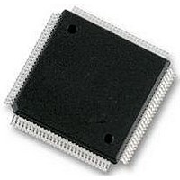
XC68HC12A0CPV8 Freescale Semiconductor, XC68HC12A0CPV8 Datasheet - Page 59

XC68HC12A0CPV8
Manufacturer Part Number
XC68HC12A0CPV8
Description
IC, 16BIT MCU, 68HC12, 8MHZ, TQFP-112
Manufacturer
Freescale Semiconductor
Datasheet
1.MC912D60ACFUE8.pdf
(460 pages)
Specifications of XC68HC12A0CPV8
Controller Family/series
68HC12
No. Of I/o's
68
Eeprom Memory Size
1KB
Ram Memory Size
2KB
Cpu Speed
8MHz
No. Of Timers
1
Core Size
16 Bit
Program Memory Size
60KB
Peripherals
ADC
Lead Free Status / RoHS Status
Lead free / RoHS Compliant
- Current page: 59 of 460
- Download datasheet (5Mb)
MC68HC912D60A — Rev. 3.1
Freescale Semiconductor
1. In 80-pin QFP package only TxCAN and RxCAN are available. PortCAN[2:7] pins should either be defined as outputs or
Port Name
PCAN[7:0]
PAD1[7:0]
PAD0[7:0]
Port CAN
Port AD1
Port AD0
PB[7:0]
PE[7:0]
PP[7:0]
PS[7:0]
PT[7:0]
PA[7:0]
have their pull-ups enabled.
Port A
Port B
Port E
Port P
Port S
Port T
72, 73
25–28,
76–80,
14–11,
80-pin
48–41
23–16
60–53
37–40
70–63
Pin Numbers
N/A
1–3
7–4
(1)
Table 3-3
84/82/80
83/81/79
108–112
/78/76/7
/77/75/7
112-pin
4/72/70
3/71/69
98–105
36–39,
18–15,
64–57
31–24
53–56
96–89
1–3
7–4
Setting the RDPT bit in the TMSK2 register configures all port T outputs
to have reduced drive levels. Levels are at normal drive capability after
reset. The TMSK2 register can be read or written anytime after reset
Refer to
,
.
MC68HC912D60A Port Description Summary
Data Direction
DDRS ($00D7)
DDRT ($00AF)
DDRA ($0002)
DDRB ($0003)
DDRE ($0009)
DDRP ($0057)
PE[7:2] In/Out
(Address)
Enhanced Capture
PE[1:0] In
Register
In/Out
In/Out
In/Out
In/Out
In/Out
In/Out
Pinout and Signal Descriptions
In
In
Port A and port B pins are used for address and data in
DDRA and DDRB are not in the address map in expanded
Analog-to-digital converter 1 and general-purpose I/O.
Analog-to-digital converter 0 and general-purpose I/O.
General purpose I/O. PCAN[1:0] are used with the
Mode selection, bus control signals and interrupt service
General-purpose I/O. PP[3:0] are used with the pulse-width
Serial communications interfaces 1 and 0 and serial
General-purpose I/O when not enabled for input capture
expanded modes. The port data registers are not in the
address map during expanded and peripheral mode
operation. When in the map, port A and port B can be
read or written any time.
or peripheral modes.
MSCAN12 module and cannot be used as I/O.
request signals; or general-purpose I/O.
modulator when enabled.
peripheral interface subsystems and general-purpose I/O.
and output compare in the timer and pulse accumulator
subsystem.
Timer.
Description
Pinout and Signal Descriptions
Technical Data
Port Signals
59
Related parts for XC68HC12A0CPV8
Image
Part Number
Description
Manufacturer
Datasheet
Request
R
Part Number:
Description:
Manufacturer:
Freescale Semiconductor, Inc
Datasheet:
Part Number:
Description:
Manufacturer:
Freescale Semiconductor, Inc
Datasheet:
Part Number:
Description:
Manufacturer:
Freescale Semiconductor, Inc
Datasheet:
Part Number:
Description:
Manufacturer:
Freescale Semiconductor, Inc
Datasheet:
Part Number:
Description:
Manufacturer:
Freescale Semiconductor, Inc
Datasheet:
Part Number:
Description:
Manufacturer:
Freescale Semiconductor, Inc
Datasheet:
Part Number:
Description:
Manufacturer:
Freescale Semiconductor, Inc
Datasheet:
Part Number:
Description:
Manufacturer:
Freescale Semiconductor, Inc
Datasheet:
Part Number:
Description:
Manufacturer:
Freescale Semiconductor, Inc
Datasheet:
Part Number:
Description:
Manufacturer:
Freescale Semiconductor, Inc
Datasheet:
Part Number:
Description:
Manufacturer:
Freescale Semiconductor, Inc
Datasheet:
Part Number:
Description:
Manufacturer:
Freescale Semiconductor, Inc
Datasheet:
Part Number:
Description:
Manufacturer:
Freescale Semiconductor, Inc
Datasheet:
Part Number:
Description:
Manufacturer:
Freescale Semiconductor, Inc
Datasheet:
Part Number:
Description:
Manufacturer:
Freescale Semiconductor, Inc
Datasheet:


