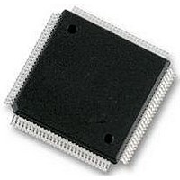
XC68HC12A0CPV8 Freescale Semiconductor, XC68HC12A0CPV8 Datasheet - Page 246

XC68HC12A0CPV8
Manufacturer Part Number
XC68HC12A0CPV8
Description
IC, 16BIT MCU, 68HC12, 8MHZ, TQFP-112
Manufacturer
Freescale Semiconductor
Datasheet
1.MC912D60ACFUE8.pdf
(460 pages)
Specifications of XC68HC12A0CPV8
Controller Family/series
68HC12
No. Of I/o's
68
Eeprom Memory Size
1KB
Ram Memory Size
2KB
Cpu Speed
8MHz
No. Of Timers
1
Core Size
16 Bit
Program Memory Size
60KB
Peripherals
ADC
Lead Free Status / RoHS Status
Lead free / RoHS Compliant
- Current page: 246 of 460
- Download datasheet (5Mb)
Enhanced Capture Timer
PACN3, PACN2 — Pulse Accumulators Count Registers
Technical Data
246
RESET:
$00A2
$00A3
BIT 7
BIt 7
Bit 7
0
6
6
6
0
PAIF — Pulse Accumulator Input edge Flag
Read: any time
Write: any time
The two 8-bit pulse accumulators PAC3 and PAC2 are cascaded to form
the PACA 16-bit pulse accumulator. When PACA in enabled (PAEN=1
in PACTL, $A0) the PACN3 and PACN2 registers contents are
respectively the high and low byte of the PACA.
When PACN3 overflows from $FF to $00, the Interrupt flag PAOVF in
PAFLG ($A1) is set.
Full count register access should take place in one clock cycle. A
separate read/write for high byte and low byte will give a different result
than accessing them as a word.
This bit is cleared automatically by a write to the PAFLG register with
bit 1 set.
Set when the selected edge is detected at the PT7 input pin. In event
mode the event edge triggers PAIF and in gated time accumulation
mode the trailing edge of the gate signal at the PT7 input pin triggers
PAIF.
This bit is cleared by a write to the PAFLG register with bit 0 set.
Any access to the PACN3, PACN2 registers will clear all the flags in
this register when TFFCA bit in register TSCR($86) is set.
5
5
5
0
Enhanced Capture Timer
4
4
4
0
3
3
3
0
2
2
2
0
MC68HC912D60A — Rev. 3.1
1
1
1
0
Freescale Semiconductor
BIT 0
Bit 0
Bit 0
0
$00A2, $00A3
PACN3 (hi)
PACN2 (lo)
Related parts for XC68HC12A0CPV8
Image
Part Number
Description
Manufacturer
Datasheet
Request
R
Part Number:
Description:
Manufacturer:
Freescale Semiconductor, Inc
Datasheet:
Part Number:
Description:
Manufacturer:
Freescale Semiconductor, Inc
Datasheet:
Part Number:
Description:
Manufacturer:
Freescale Semiconductor, Inc
Datasheet:
Part Number:
Description:
Manufacturer:
Freescale Semiconductor, Inc
Datasheet:
Part Number:
Description:
Manufacturer:
Freescale Semiconductor, Inc
Datasheet:
Part Number:
Description:
Manufacturer:
Freescale Semiconductor, Inc
Datasheet:
Part Number:
Description:
Manufacturer:
Freescale Semiconductor, Inc
Datasheet:
Part Number:
Description:
Manufacturer:
Freescale Semiconductor, Inc
Datasheet:
Part Number:
Description:
Manufacturer:
Freescale Semiconductor, Inc
Datasheet:
Part Number:
Description:
Manufacturer:
Freescale Semiconductor, Inc
Datasheet:
Part Number:
Description:
Manufacturer:
Freescale Semiconductor, Inc
Datasheet:
Part Number:
Description:
Manufacturer:
Freescale Semiconductor, Inc
Datasheet:
Part Number:
Description:
Manufacturer:
Freescale Semiconductor, Inc
Datasheet:
Part Number:
Description:
Manufacturer:
Freescale Semiconductor, Inc
Datasheet:
Part Number:
Description:
Manufacturer:
Freescale Semiconductor, Inc
Datasheet:


