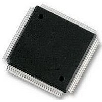
XC68HC12A0CPV8 Freescale Semiconductor, XC68HC12A0CPV8 Datasheet - Page 275

XC68HC12A0CPV8
Manufacturer Part Number
XC68HC12A0CPV8
Description
IC, 16BIT MCU, 68HC12, 8MHZ, TQFP-112
Manufacturer
Freescale Semiconductor
Datasheet
1.MC912D60ACFUE8.pdf
(460 pages)
Specifications of XC68HC12A0CPV8
Controller Family/series
68HC12
No. Of I/o's
68
Eeprom Memory Size
1KB
Ram Memory Size
2KB
Cpu Speed
8MHz
No. Of Timers
1
Core Size
16 Bit
Program Memory Size
60KB
Peripherals
ADC
Lead Free Status / RoHS Status
Lead free / RoHS Compliant
- Current page: 275 of 460
- Download datasheet (5Mb)
SC0DRH/SC1DRH — SCI Data Register High
SC0DRL/SC1DRL — SCI Data Register Low
MC68HC912D60A — Rev. 3.1
Freescale Semiconductor
RESET:
RESET:
R7/T7
Bit 7
Bit 7
R8
—
—
R6/T6
T8
—
—
6
6
R8 — Receive Bit 8
T8 — Transmit Bit 8
R7/T7–R0/T0 — Receive/Transmit Data Bits 7 to 0
Read anytime. Write has no meaning or affect.
This bit is the ninth serial data bit received when the SCI system is
configured for nine-data-bit operation.
Read or write anytime.
This bit is the ninth serial data bit transmitted when the SCI system is
configured for nine-data-bit operation. When using 9-bit data format
this bit does not have to be written for each data word. The same
value will be transmitted as the ninth bit until this bit is rewritten.
Reads access the eight bits of the read-only SCI receive data register
(RDR). Writes access the eight bits of the write-only SCI transmit data
register (TDR). SCxDRL:SCxDRH form the 9-bit data word for the
SCI. If the SCI is being used with a 7- or 8-bit data word, only SCxDRL
needs to be accessed. If a 9-bit format is used, the upper register
should be written first to ensure that it is transferred to the transmitter
shift register with the lower register.
R5/T5
—
—
5
0
5
Multiple Serial Interface
R4/T4
—
—
4
4
0
R3/T3
—
—
3
0
3
R2/T2
—
—
2
2
0
Serial Communication Interface (SCI)
R1/T1
—
—
1
0
1
Multiple Serial Interface
R0/T0
Bit 0
Bit 0
—
—
0
Technical Data
$00C6/$00CE
$00C7/$00CF
275
Related parts for XC68HC12A0CPV8
Image
Part Number
Description
Manufacturer
Datasheet
Request
R
Part Number:
Description:
Manufacturer:
Freescale Semiconductor, Inc
Datasheet:
Part Number:
Description:
Manufacturer:
Freescale Semiconductor, Inc
Datasheet:
Part Number:
Description:
Manufacturer:
Freescale Semiconductor, Inc
Datasheet:
Part Number:
Description:
Manufacturer:
Freescale Semiconductor, Inc
Datasheet:
Part Number:
Description:
Manufacturer:
Freescale Semiconductor, Inc
Datasheet:
Part Number:
Description:
Manufacturer:
Freescale Semiconductor, Inc
Datasheet:
Part Number:
Description:
Manufacturer:
Freescale Semiconductor, Inc
Datasheet:
Part Number:
Description:
Manufacturer:
Freescale Semiconductor, Inc
Datasheet:
Part Number:
Description:
Manufacturer:
Freescale Semiconductor, Inc
Datasheet:
Part Number:
Description:
Manufacturer:
Freescale Semiconductor, Inc
Datasheet:
Part Number:
Description:
Manufacturer:
Freescale Semiconductor, Inc
Datasheet:
Part Number:
Description:
Manufacturer:
Freescale Semiconductor, Inc
Datasheet:
Part Number:
Description:
Manufacturer:
Freescale Semiconductor, Inc
Datasheet:
Part Number:
Description:
Manufacturer:
Freescale Semiconductor, Inc
Datasheet:
Part Number:
Description:
Manufacturer:
Freescale Semiconductor, Inc
Datasheet:


