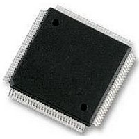
XC68HC12A0CPV8 Freescale Semiconductor, XC68HC12A0CPV8 Datasheet - Page 282

XC68HC12A0CPV8
Manufacturer Part Number
XC68HC12A0CPV8
Description
IC, 16BIT MCU, 68HC12, 8MHZ, TQFP-112
Manufacturer
Freescale Semiconductor
Datasheet
1.MC912D60ACFUE8.pdf
(460 pages)
Specifications of XC68HC12A0CPV8
Controller Family/series
68HC12
No. Of I/o's
68
Eeprom Memory Size
1KB
Ram Memory Size
2KB
Cpu Speed
8MHz
No. Of Timers
1
Core Size
16 Bit
Program Memory Size
60KB
Peripherals
ADC
Lead Free Status / RoHS Status
Lead free / RoHS Compliant
- Current page: 282 of 460
- Download datasheet (5Mb)
Multiple Serial Interface
SP0CR2 — SPI Control Register 2
Technical Data
282
RESET:
Bit 7
0
0
1. The serial pin control 0 bit enables bidirectional configurations.
2. Slave output is enabled if DDS4 = 1, SS = 0 and MSTR = 0. (#1, #3)
3. Master output is enabled if DDS5 = 1 and MSTR = 1. (#2, #4)
4. SCK output is enabled if DDS6 = 1 and MSTR = 1. (#2, #4)
5. SS output is enabled if DDS7 = 1, SSOE = 1 and MSTR = 1. (#2, #4)
#1
#2
#3
#4
Pin Mode
Bidirectional
6
0
0
Read or write anytime.
SPSWAI — Serial Interface Stop in WAIT mode
SPC0 — Serial Pin Control 0
Normal
Normally data is transferred most significant bit first.This bit does not
affect the position of the MSB and LSB in the data register. Reads and
writes of the data register will always have MSB in bit 7.
This bit decides serial pin configurations with MSTR control bit.
0 = Serial interface clock operates normally
1 = Halt serial interface clock generation in WAIT mode
5
0
0
SPC0
Multiple Serial Interface
0
1
(1)
4
0
0
MSTR
0
1
0
1
3
0
0
Slave Out
Master In Master Out
Slave I/O
MISO
GPI/O
(2)
2
0
0
Master I/O
MOSI
Slave In
GPI/O
SPSWAI
MC68HC912D60A — Rev. 3.1
(3)
1
0
Freescale Semiconductor
SCK Out
SCK Out
SCK In
SCK In
SCK
SPC0
Bit 0
0
(4)
SS I/O
SS I/O
SS In
SS In
SS
$00D1
(5)
Related parts for XC68HC12A0CPV8
Image
Part Number
Description
Manufacturer
Datasheet
Request
R
Part Number:
Description:
Manufacturer:
Freescale Semiconductor, Inc
Datasheet:
Part Number:
Description:
Manufacturer:
Freescale Semiconductor, Inc
Datasheet:
Part Number:
Description:
Manufacturer:
Freescale Semiconductor, Inc
Datasheet:
Part Number:
Description:
Manufacturer:
Freescale Semiconductor, Inc
Datasheet:
Part Number:
Description:
Manufacturer:
Freescale Semiconductor, Inc
Datasheet:
Part Number:
Description:
Manufacturer:
Freescale Semiconductor, Inc
Datasheet:
Part Number:
Description:
Manufacturer:
Freescale Semiconductor, Inc
Datasheet:
Part Number:
Description:
Manufacturer:
Freescale Semiconductor, Inc
Datasheet:
Part Number:
Description:
Manufacturer:
Freescale Semiconductor, Inc
Datasheet:
Part Number:
Description:
Manufacturer:
Freescale Semiconductor, Inc
Datasheet:
Part Number:
Description:
Manufacturer:
Freescale Semiconductor, Inc
Datasheet:
Part Number:
Description:
Manufacturer:
Freescale Semiconductor, Inc
Datasheet:
Part Number:
Description:
Manufacturer:
Freescale Semiconductor, Inc
Datasheet:
Part Number:
Description:
Manufacturer:
Freescale Semiconductor, Inc
Datasheet:
Part Number:
Description:
Manufacturer:
Freescale Semiconductor, Inc
Datasheet:


