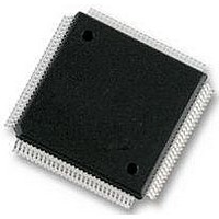
XC68HC12A0CPV8 Freescale Semiconductor, XC68HC12A0CPV8 Datasheet - Page 365

XC68HC12A0CPV8
Manufacturer Part Number
XC68HC12A0CPV8
Description
IC, 16BIT MCU, 68HC12, 8MHZ, TQFP-112
Manufacturer
Freescale Semiconductor
Datasheet
1.MC912D60ACFUE8.pdf
(460 pages)
Specifications of XC68HC12A0CPV8
Controller Family/series
68HC12
No. Of I/o's
68
Eeprom Memory Size
1KB
Ram Memory Size
2KB
Cpu Speed
8MHz
No. Of Timers
1
Core Size
16 Bit
Program Memory Size
60KB
Peripherals
ADC
Lead Free Status / RoHS Status
Lead free / RoHS Compliant
- Current page: 365 of 460
- Download datasheet (5Mb)
MC68HC912D60A — Rev. 3.1
Freescale Semiconductor
RES10 — A/D Resolution Select
SMP[1:0] — Sample Time Select
PRS[4:0] — ATD Clock Prescaler
This bit determines the resolution of the A/D converter: 8-bits or 10-
bits. The A/D converter has the accuracy of a 10-bit converter.
However, if low resolution is adequate, the conversion can be
speeded up by selecting 8-bit resolution.
These two bits select the length of the third phase of the sample
period (in internal ATD clock cycles) which occurs after the buffered
sample and transfer. During this phase, the external analog signal is
connected directly to the storage node for final charging and improved
accuracy. Note that the ATD clock period is itself a function of the
prescaler value (bits PRS0–4).
for the third sample phase.
The binary prescaler value (0 to 31) plus one (1 to 32) becomes the
divide-by-factor for a modulus counter used to prescale the system
PCLK frequency. The resulting scaled clock is further divided by 2
before the ATD internal clock is generated. This clock is used to drive
the S/H and A/D machines.
Note that the maximum ATD clock frequency is half of the system
clock. The default prescaler value is 00001 which results in a default
ATD clock frequency that is quarter of the system clock i.e. with 8MHz
bus the ATD module clock is 2MHz.
by operation and the appropriate range of system clock frequencies.
0 = 8-bit resolution selected
1 = 10-bit resolution selected
Analog-to-Digital Converter
Table 18-4. Final Sample Time Selection
SMP1
0
0
1
1
SMP0
0
1
0
1
Table 18-4
16 A/D clock periods
Final Sample Time
2 A/D clock periods
4 A/D clock periods
8 A/D clock periods
Table 18-5
lists the lengths available
Analog-to-Digital Converter
illustrates the divide-
Technical Data
ATD Registers
365
Related parts for XC68HC12A0CPV8
Image
Part Number
Description
Manufacturer
Datasheet
Request
R
Part Number:
Description:
Manufacturer:
Freescale Semiconductor, Inc
Datasheet:
Part Number:
Description:
Manufacturer:
Freescale Semiconductor, Inc
Datasheet:
Part Number:
Description:
Manufacturer:
Freescale Semiconductor, Inc
Datasheet:
Part Number:
Description:
Manufacturer:
Freescale Semiconductor, Inc
Datasheet:
Part Number:
Description:
Manufacturer:
Freescale Semiconductor, Inc
Datasheet:
Part Number:
Description:
Manufacturer:
Freescale Semiconductor, Inc
Datasheet:
Part Number:
Description:
Manufacturer:
Freescale Semiconductor, Inc
Datasheet:
Part Number:
Description:
Manufacturer:
Freescale Semiconductor, Inc
Datasheet:
Part Number:
Description:
Manufacturer:
Freescale Semiconductor, Inc
Datasheet:
Part Number:
Description:
Manufacturer:
Freescale Semiconductor, Inc
Datasheet:
Part Number:
Description:
Manufacturer:
Freescale Semiconductor, Inc
Datasheet:
Part Number:
Description:
Manufacturer:
Freescale Semiconductor, Inc
Datasheet:
Part Number:
Description:
Manufacturer:
Freescale Semiconductor, Inc
Datasheet:
Part Number:
Description:
Manufacturer:
Freescale Semiconductor, Inc
Datasheet:
Part Number:
Description:
Manufacturer:
Freescale Semiconductor, Inc
Datasheet:


