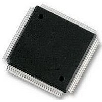
XC68HC12A0CPV8 Freescale Semiconductor, XC68HC12A0CPV8 Datasheet - Page 364

XC68HC12A0CPV8
Manufacturer Part Number
XC68HC12A0CPV8
Description
IC, 16BIT MCU, 68HC12, 8MHZ, TQFP-112
Manufacturer
Freescale Semiconductor
Datasheet
1.MC912D60ACFUE8.pdf
(460 pages)
Specifications of XC68HC12A0CPV8
Controller Family/series
68HC12
No. Of I/o's
68
Eeprom Memory Size
1KB
Ram Memory Size
2KB
Cpu Speed
8MHz
No. Of Timers
1
Core Size
16 Bit
Program Memory Size
60KB
Peripherals
ADC
Lead Free Status / RoHS Status
Lead free / RoHS Compliant
- Current page: 364 of 460
- Download datasheet (5Mb)
ATD0CTL4/ATD1CTL4 — ATD Control Register 4
Analog-to-Digital Converter
18.9.3 ATDCTL4 ATD Control Register 4
Technical Data
364
RESET:
RES10
Bit 7
0
SMP1
6
0
FRZ1, FRZ0 — Background Debug Freeze Enable
ATD control register 4 is used to select the internal ATD clock frequency
(based on the system clock), select the length of the third phase of the
sample period, and set the resolution of the A/D conversion (i.e. 8-bits or
10-bits). All writes to this register have an immediate effect. If a
conversion is in progress, the entire conversion sequence is aborted. A
write to this register (or ATDCTL5) initiates a new conversion sequence.
Finally, which result registers hold valid data can be tracked using the
conversion complete flags. Fast flag clear mode may or may not be
useful in a particular application to track valid data.
Background debug freeze function allows the ATD module to pause
when a breakpoint is encountered.
FRZ0 determine the ATD’s response to a breakpoint. When BDM is
deasserted, the ATD module continues operating as it was before the
breakpoint occurred.
Table 18-3. ATD Response to Background Debug Enable
SMP0
FRZ1
5
0
0
0
1
1
Analog-to-Digital Converter
FRZ0
PRS4
0
1
0
1
4
0
Continue conversions in active background mode
PRS3
3
0
Finish current conversion, then freeze
Freeze when BDM is active
PRS2
Table 18-3
2
0
ATD Response
Reserved
PRS1
MC68HC912D60A — Rev. 3.1
1
0
shows how FRZ1 and
Freescale Semiconductor
PRS0
Bit 0
1
$0064/$01E4
Related parts for XC68HC12A0CPV8
Image
Part Number
Description
Manufacturer
Datasheet
Request
R
Part Number:
Description:
Manufacturer:
Freescale Semiconductor, Inc
Datasheet:
Part Number:
Description:
Manufacturer:
Freescale Semiconductor, Inc
Datasheet:
Part Number:
Description:
Manufacturer:
Freescale Semiconductor, Inc
Datasheet:
Part Number:
Description:
Manufacturer:
Freescale Semiconductor, Inc
Datasheet:
Part Number:
Description:
Manufacturer:
Freescale Semiconductor, Inc
Datasheet:
Part Number:
Description:
Manufacturer:
Freescale Semiconductor, Inc
Datasheet:
Part Number:
Description:
Manufacturer:
Freescale Semiconductor, Inc
Datasheet:
Part Number:
Description:
Manufacturer:
Freescale Semiconductor, Inc
Datasheet:
Part Number:
Description:
Manufacturer:
Freescale Semiconductor, Inc
Datasheet:
Part Number:
Description:
Manufacturer:
Freescale Semiconductor, Inc
Datasheet:
Part Number:
Description:
Manufacturer:
Freescale Semiconductor, Inc
Datasheet:
Part Number:
Description:
Manufacturer:
Freescale Semiconductor, Inc
Datasheet:
Part Number:
Description:
Manufacturer:
Freescale Semiconductor, Inc
Datasheet:
Part Number:
Description:
Manufacturer:
Freescale Semiconductor, Inc
Datasheet:
Part Number:
Description:
Manufacturer:
Freescale Semiconductor, Inc
Datasheet:


