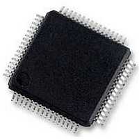
UPD78F0890GK(A)-GAJ-AX NEC, UPD78F0890GK(A)-GAJ-AX Datasheet - Page 50

UPD78F0890GK(A)-GAJ-AX
Manufacturer Part Number
UPD78F0890GK(A)-GAJ-AX
Description
8BIT MCU, 128K FLASH, 7K RAM, LQFP
Manufacturer
NEC
Datasheet
1.UPD78F0890GKA-GAJ-AX.pdf
(732 pages)
Specifications of UPD78F0890GK(A)-GAJ-AX
Controller Family/series
UPD78F
No. Of I/o's
55
Ram Memory Size
7KB
Cpu Speed
20MHz
No. Of Timers
10
No. Of Pwm
RoHS Compliant
Core Size
8bit
Program Memory Size
128KB
Oscillator Type
External, Internal
- Current page: 50 of 732
- Download datasheet (4Mb)
memory.
50
(b)
The following table shows the relations among bank numbers, CPU addresses, and real addresses of the flash
μ
PD78F0890
(a)
(b)
μ
μ
PD78F0889
PD78F0890
B F F F H
7 F F F H
8 0 0 0 H
0 0 0 0 H
Table 3-5. Bank Numbers, CPU Addresses, and Real Addresses of Flash Memory
4 or more
6 or more
Bank No.
Bank No.
−
0
1
2
3
−
0
1
2
3
4
5
Bank
area 0
16384
8 bits
Bank
area 1
16384
8 bits
CHAPTER 3 CPU ARCHITECTURE
0000H to 7FFFH (common area)
8000H to BFFFH
Setting prohibited
0000H to 7FFFH (common area)
8000H to BFFFH
Setting prohibited
User’s Manual U17554EJ4V0UD
CPU Address
CPU Address
Bank
area 2
16384
8 bits
Common area
32768
8 bits
Bank
area 3
16384
8 bits
00000H to 07FFFH
08000H to 0BFFFH
0C000H to 0FFFFH
10000H to 13FFFH
14000H to 17FFFH
00000H to 07FFFH
08000H to 0BFFFH
0C000H to 0FFFFH
10000H to 13FFFH
14000H to 17FFFH
18000H to 1BFFFH
1C000H to 1FFFFH
Real Address of Flash Memory
Real Address of Flash Memory
Bank
area 4
16384
8 bits
Bank
area 5
16384
8 bits
Related parts for UPD78F0890GK(A)-GAJ-AX
Image
Part Number
Description
Manufacturer
Datasheet
Request
R

Part Number:
Description:
16/8 bit single-chip microcomputer
Manufacturer:
NEC
Datasheet:

Part Number:
Description:
Dual audio power amp circuit
Manufacturer:
NEC
Datasheet:

Part Number:
Description:
Dual comparator
Manufacturer:
NEC
Datasheet:

Part Number:
Description:
MOS type composite field effect transistor
Manufacturer:
NEC
Datasheet:

Part Number:
Description:
50 V/100 mA FET array incorporating 2 N-ch MOSFETs
Manufacturer:
NEC
Datasheet:

Part Number:
Description:
6-pin small MM high-frequency double transistor
Manufacturer:
NEC
Datasheet:

Part Number:
Description:
6-pin small MM high-frequency double transistor
Manufacturer:
NEC
Datasheet:

Part Number:
Description:
6-pin small MM high-frequency double transistor
Manufacturer:
NEC
Datasheet:

Part Number:
Description:
6-pin small MM high-frequency double transistor
Manufacturer:
NEC
Datasheet:

Part Number:
Description:
Twin transistors equipped with different model chips(6P small MM)
Manufacturer:
NEC
Datasheet:

Part Number:
Description:
Bipolar analog integrated circuit
Manufacturer:
NEC
Datasheet:


