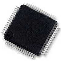
UPD78F0890GK(A)-GAJ-AX NEC, UPD78F0890GK(A)-GAJ-AX Datasheet - Page 45

UPD78F0890GK(A)-GAJ-AX
Manufacturer Part Number
UPD78F0890GK(A)-GAJ-AX
Description
8BIT MCU, 128K FLASH, 7K RAM, LQFP
Manufacturer
NEC
Datasheet
1.UPD78F0890GKA-GAJ-AX.pdf
(732 pages)
Specifications of UPD78F0890GK(A)-GAJ-AX
Controller Family/series
UPD78F
No. Of I/o's
55
Ram Memory Size
7KB
Cpu Speed
20MHz
No. Of Timers
10
No. Of Pwm
RoHS Compliant
Core Size
8bit
Program Memory Size
128KB
Oscillator Type
External, Internal
- Current page: 45 of 732
- Download datasheet (4Mb)
Notes 1.
Remark The flash memory is divided into blocks (one block = 1 KB). For the address values and block numbers,
Bank
area
Common
area
2.
3.
4.
Data memory
space
see Table 3-2 Correspondence Between Address Values and Block Numbers in Flash Memory.
RAM space in
which instruction
can be fetched
During on-chip debugging, use of this area is disabled since it is used as the user data backup area for
communication.
During on-chip debugging, use of this area is disabled since it is used as the communication command
area (269 bytes).
When boot swap is not used: Set the option bytes to 0080H to 0084H.
When boot swap is used:
Writing boot cluster 0 can be prohibited depending on the setting of security (see 24.8
Setting).
Program
memory space
1 KB
B B F F H
B F F F H
B C 0 0 H
7 F F F H
7 C 0 0 H
7 B F F H
8 4 F F H
8 3 F F H
8 0 0 0 H
0 7 F F H
0 4 0 0 H
0 3 F F H
0 0 0 0 H
FAFFH
FFFFH
FF00H
FEFFH
FEE0H
FEDFH
FB00H
FA00H
F9FFH
F800H
F7FFH
DFFFH
C000H
BFFFH
E000H
7FFFH
0190H
018FH
0083H
0082H
0000H
8000H
Block 2FH
Block 20H
Block 1FH
Block 01H
Block 00H
(Memory bank 0)
Internal high-speed RAM
Internal expansion RAM
General-purpose
Special function
32 × 8 bits
registers (SFR)
16384 × 8 bits
Flash memory
Flash memory
registers
6144 × 8 bits
32768 × 8 bits
1024 × 8 bits
AFCAN area
256 × 8 bits
256 × 8 bits
Reserved
Reserved
(common)
(bank 0)
Note 1
Note 2
Figure 3-4. Memory Map (
CHAPTER 3 CPU ARCHITECTURE
Set the option bytes to 0080H to 0084H and 1080H to 1084H.
User’s Manual U17554EJ4V0UD
Block 3FH
Block 30H
16384 × 8 bits
16384 × 8 bits
(Memory bank 1)
FF1FH
FF20H
FE1FH
FE0FH
FE20H
FE10H
(bank 2)
(bank 1)
16384 × 8 bits
16384 × 8 bits
(bank 3)
(bank 4)
Short direct
addressing
16384 × 8 bits
(bank 5)
7 F F F H
1 0 7 F H
0 F F F H
0 7 F F H
μ
1 0 8 5 H
1 0 8 4 H
1 0 8 0 H
1 0 0 0 H
0 8 0 0 H
0 0 7 F H
0 0 3 F H
0 0 8 5 H
0 0 8 4 H
0 0 8 0 H
0 0 4 0 H
0 0 0 0 H
PD78F0890)
Block 4FH
Block 40H
(Memory bank 2)
Option byte area
Option byte area
CALLF entry area
CALLT table area
Vector table area
Program area
Program area
Program area
2048
1915
64
64
5
5
8 bits
8 bits
8 bits
8 bits
8 bits
8 bits
Note 3
Note 3
. . .
1 F F F H
Boot cluster 0
Boot cluster 1
Block 7FH
Block 70H
(Memory bank 5)
Note 4
Security
45
Related parts for UPD78F0890GK(A)-GAJ-AX
Image
Part Number
Description
Manufacturer
Datasheet
Request
R

Part Number:
Description:
16/8 bit single-chip microcomputer
Manufacturer:
NEC
Datasheet:

Part Number:
Description:
Dual audio power amp circuit
Manufacturer:
NEC
Datasheet:

Part Number:
Description:
Dual comparator
Manufacturer:
NEC
Datasheet:

Part Number:
Description:
MOS type composite field effect transistor
Manufacturer:
NEC
Datasheet:

Part Number:
Description:
50 V/100 mA FET array incorporating 2 N-ch MOSFETs
Manufacturer:
NEC
Datasheet:

Part Number:
Description:
6-pin small MM high-frequency double transistor
Manufacturer:
NEC
Datasheet:

Part Number:
Description:
6-pin small MM high-frequency double transistor
Manufacturer:
NEC
Datasheet:

Part Number:
Description:
6-pin small MM high-frequency double transistor
Manufacturer:
NEC
Datasheet:

Part Number:
Description:
6-pin small MM high-frequency double transistor
Manufacturer:
NEC
Datasheet:

Part Number:
Description:
Twin transistors equipped with different model chips(6P small MM)
Manufacturer:
NEC
Datasheet:

Part Number:
Description:
Bipolar analog integrated circuit
Manufacturer:
NEC
Datasheet:


