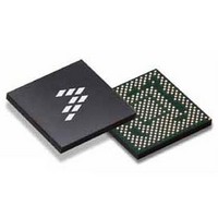
SC900841JVKR2 Freescale Semiconductor, SC900841JVKR2 Datasheet - Page 93

SC900841JVKR2
Manufacturer Part Number
SC900841JVKR2
Description
IC POWER MGT 338-MAPBGA
Manufacturer
Freescale Semiconductor
Specifications of SC900841JVKR2
Applications
PC's, PDA's
Operating Temperature
-40°C ~ 85°C
Mounting Type
Surface Mount
Package / Case
338-TBGA
Input Voltage
2.8 V to 4.4 V
Maximum Operating Temperature
+ 85 C
Minimum Operating Temperature
- 40 C
Lead Free Status / RoHS Status
Lead free / RoHS Compliant
Current - Supply
-
Voltage - Supply
-
Lead Free Status / Rohs Status
Lead free / RoHS Compliant
Available stocks
Company
Part Number
Manufacturer
Quantity
Price
Company:
Part Number:
SC900841JVKR2
Manufacturer:
Freescale Semiconductor
Quantity:
10 000
- Current page: 93 of 192
- Download datasheet (8Mb)
VPNL18
with a P-CH Pass FET. It is high performance, low noise, and
high PSRR, with a low quiescent current and fast transient
response. VPNL18 is actively discharged during shutdown.
Main Features
• Uses V21 as the main power supply
• 225 mA maximum continuous output current
• Optimized for a 2.2 µF external filter capacitor with a
Table 47. VCC180CNT Register Structure and Bits Description
Table 48. VPNL18 Control Register Structure and Bits Description
Analog Integrated Circuit Device Data
Freescale Semiconductor
AOACCTLVCC180
AOACCTLVPANEL18
VPNL18 is a low drop-out (LDO) fully integrated regulator
maximum of 10 mΩ ESR
CTLVPANEL18
Reserved
Reserved
Name
( Shared with VCC180 and VPMIC)
( Shared with VCC180 and VPMIC)
5:3
7:6
V
OPNL18
Bits
2:0
5:3
7:6
VCC180 State Control during AOAC Exit (when the Exit pin is EXITSTBY pin is asserted). These bits will be
initialized by the system SPI controller after power up.
X0 = Do not copy
x1 = Do not copy
x2 = Do not copy
x3 = Do not copy
Reserved
VOUTPNL18
VPNL18 State Control
x0 = Reserved
x1 = Reserved
x2 = Reserved
x3 = Reserved
VPNL18 State Control during AOAC Exit (when the Exit pin is EXITSTBY pin is asserted). These bits will be
initialized by the system SPI controller after power up.
X0 = Do not copy
x1 = Do not copy
x2 = Do not copy
x3 = Do not copy
Reserved
C
OPNL18
PVIN 2P1
GND2P1
Figure 45. VPNL18 Detailed Internal Block Diagram
VPANEL18CNT (ADDR 0x46 - R/W - Default value: 0x24)
Discharge
V
I
OPNL18
OPNL18
Controller
Z
Output Monitor
_
+
reference ground pin (GND2P1) with VCC180 and VPMIC
regulators, yet each has independent control. PVIN2P1 is
supplied from the V21 voltage.
V
• Uses an internal pass FET
• The output for each LDO is monitored for over-current
VPNL18 Status/Control Registers and Bits Description
REF
VPNL18 shares an input voltage pin (PVIN2P1) and a
conditions and under-voltage events
Description
x4 = OFF
x5 = Low Power
x6 = Active
x7 = Active
AOACCTLVPNL18
x4 = OFF
x5 = Low Power
x6 = Active
x7 = Active
x4 = OFF
x5 = Low Power
x6 = Active
x7 = Active
VPNL18FAULT
CTLVPNL18
FUNCTIONAL DEVICE OPERATION
Interface
SPI
POWER SUPPLIES
900841
93
Related parts for SC900841JVKR2
Image
Part Number
Description
Manufacturer
Datasheet
Request
R
Part Number:
Description:
Ultra-mobile Platform Pmic
Manufacturer:
Freescale Semiconductor, Inc
Datasheet:

Part Number:
Description:
Sc900 Programmable Penta Uldo With Reset And I2c Interface
Manufacturer:
Semtech Corporation
Datasheet:
Part Number:
Description:
Manufacturer:
Freescale Semiconductor, Inc
Datasheet:
Part Number:
Description:
Manufacturer:
Freescale Semiconductor, Inc
Datasheet:
Part Number:
Description:
Manufacturer:
Freescale Semiconductor, Inc
Datasheet:
Part Number:
Description:
Manufacturer:
Freescale Semiconductor, Inc
Datasheet:
Part Number:
Description:
Manufacturer:
Freescale Semiconductor, Inc
Datasheet:
Part Number:
Description:
Manufacturer:
Freescale Semiconductor, Inc
Datasheet:
Part Number:
Description:
Manufacturer:
Freescale Semiconductor, Inc
Datasheet:
Part Number:
Description:
Manufacturer:
Freescale Semiconductor, Inc
Datasheet:
Part Number:
Description:
Manufacturer:
Freescale Semiconductor, Inc
Datasheet:
Part Number:
Description:
Manufacturer:
Freescale Semiconductor, Inc
Datasheet:
Part Number:
Description:
Manufacturer:
Freescale Semiconductor, Inc
Datasheet:
Part Number:
Description:
Manufacturer:
Freescale Semiconductor, Inc
Datasheet:
Part Number:
Description:
Manufacturer:
Freescale Semiconductor, Inc
Datasheet:


