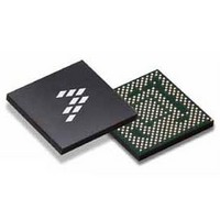
SC900841JVKR2 Freescale Semiconductor, SC900841JVKR2 Datasheet - Page 55

SC900841JVKR2
Manufacturer Part Number
SC900841JVKR2
Description
IC POWER MGT 338-MAPBGA
Manufacturer
Freescale Semiconductor
Specifications of SC900841JVKR2
Applications
PC's, PDA's
Operating Temperature
-40°C ~ 85°C
Mounting Type
Surface Mount
Package / Case
338-TBGA
Input Voltage
2.8 V to 4.4 V
Maximum Operating Temperature
+ 85 C
Minimum Operating Temperature
- 40 C
Lead Free Status / RoHS Status
Lead free / RoHS Compliant
Current - Supply
-
Voltage - Supply
-
Lead Free Status / Rohs Status
Lead free / RoHS Compliant
Available stocks
Company
Part Number
Manufacturer
Quantity
Price
Company:
Part Number:
SC900841JVKR2
Manufacturer:
Freescale Semiconductor
Quantity:
10 000
alarm bytes must use the same data mode, either binary or
BCD. Both the alarm hours, and the hours bytes must use the
same hours format, either 12 or 24.
initialized, the real-time clock makes all updates in the selected
data mode. The data mode (DM) cannot be changed without
re-initializing the 10 data bytes.
Reading the Time, Calendar, and Alarm
read by accessing the RTC registers through the system SPI.
Since the alarm is only updated by a SPI write instruction, the
three alarm registers may be read at any time and will always
be defined.
individual SPI read transaction requires 25 cycles (less for
burst-read). The RTC contains seven timekeeping registers to
keep track of seconds, minutes, hours, day-of-week, day-of-
month, month, and year. If the SPI is clocked at the slowest
frequency, and the RTC is read using individual (not burst) SPI
read commands, the following equation gives the maximum
amount of time it takes the processor to read a complete date
and time (assuming the reads are done sequentially, and
uninterrupted): (25 * 7) / (12.5 MHz) = 14 μs.
accesses the time and date information will find the data in
transition statistically 14 times per million attempts. If a clock
update occurs during the time it takes to read all seven
timekeeping registers, the values read may be inconsistent. In
Table 23. Time, Calendar, and Alarm Data Modes
Analog Integrated Circuit Device Data
Freescale Semiconductor
Notes
Address
location
20.
The Set bit may now be cleared to allow updates. Once
Under normal operation, the current time and date may be
This equation shows that a program which randomly
The 900841 SPI will run at a minimum of 12.5 MHz. Each
0x10
0x11
0x12
0x13
0x14
0x15
0x16
0x17
0x18
0x19
Example: 11:58:21 Thursday 15 February 2008 (time is AM)
Date of the Month
Day of the Week
(12 Hour Mode)
(24 Hour Mode)
(12 Hour Mode)
(24 Hour Mode)
Seconds Alarm
Minutes Alarm
Hours Alarm
Sunday=1
Function
Seconds
Minutes
Month
Hours
Year
Decimal
Range
0-59
0-59
0-59
0-59
1-12
0-23
1-12
0-23
1-31
1-12
0-99
1-7
$01-$0C(AM) / $81-$92(PM)
$01-$0C(AM) / $81-$92(PM)
Binary Data Mode
$00-$3B
$00-$3B
$00-$3B
$00-$3B
$01-$0C
$00-$17
$00-$17
$01-$07
$01-$1F
$00-$63
locations represent 1-to-12 or 0-to-23. When the 12 hour
format is selected the high order bit of the hour bytes
represents PM when it is a "1". The 24/12 bit cannot be
changed without re-initializing the hour and alarm-hour
locations.
calendar, and alarm locations.
other words, if the program starts to read the seven date/time
registers and an RTC update occurs, the data collected may be
in transition. In this event, it is possible to read transition data
in one of the registers, resulting in undefined output. It is more
likely that the registers read after the update would be
incremented (by one second), and the registers read before the
update would not.
by the processor program. Once per second the seven bytes
are advanced by one second and checked for an alarm
condition. If any of the seven bytes are read at this time, the
data outputs should be considered undefined. Similarly, all
seven bytes should be read between updates to get a
consistent time and date. Reading some of the bytes before an
update and some after, may result in an erroneous output. The
Update Cycle
update cycle in the processor program.
Update Cycle
second, assuming one of the proper time bases is in place and
The 24/12 bit in Register B establishes whether the hour
Table 23
The time, calendar, and alarm bytes are always accessible
The RTC module executes an update cycle once per
Range
$01-$12(AM) / $81-$92(PM)
$01-$12(AM) / $81-$92(PM)
CLOCK GENERATION AND REAL TIME CLOCK (RTC)
shows the binary and BCD formats of the 10 time,
section explains how to accommodate the
BCD Data Mode
$00-$59
$00-$59
$00-$59
$00-$59
$00-$23
$00-$23
$01-$07
$01-$31
$01-$12
$00-$99
FUNCTIONAL DEVICE OPERATION
Binary Data
Mode
3A
3A
0B
0B
0F
15
15
05
02
08
Example
BCD Data
(20)
Mode
21
21
58
58
11
11
05
15
02
08
900841
55


