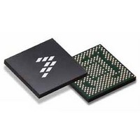
SC900841JVKR2 Freescale Semiconductor, SC900841JVKR2 Datasheet - Page 48

SC900841JVKR2
Manufacturer Part Number
SC900841JVKR2
Description
IC POWER MGT 338-MAPBGA
Manufacturer
Freescale Semiconductor
Specifications of SC900841JVKR2
Applications
PC's, PDA's
Operating Temperature
-40°C ~ 85°C
Mounting Type
Surface Mount
Package / Case
338-TBGA
Input Voltage
2.8 V to 4.4 V
Maximum Operating Temperature
+ 85 C
Minimum Operating Temperature
- 40 C
Lead Free Status / RoHS Status
Lead free / RoHS Compliant
Current - Supply
-
Voltage - Supply
-
Lead Free Status / Rohs Status
Lead free / RoHS Compliant
Available stocks
Company
Part Number
Manufacturer
Quantity
Price
Company:
Part Number:
SC900841JVKR2
Manufacturer:
Freescale Semiconductor
Quantity:
10 000
- Current page: 48 of 192
- Download datasheet (8Mb)
the VCCP, VCCPDDR, VCCA, and VCC180 rails are to be
turned on by the assertion of the EXITSTBY signal. However,
every regulator has an AOACCTLVxx register setting, and
can be configured to turn on, turn off, or have no change. The
power-on default AOACCTLVxx register setting for all other
regulators is set to no change. Note that the VDDQ regulator
has to be enabled in order for the VCCA regulator to turn on.
THERMTRIPB Pin
It is asserted by the CPU to indicate a catastrophic thermal
event. On the falling edge of THERMTRIPB, the PMIC has
500 ms to sequence off all rails from the highest to lowest.
The PMIC will turn on automatically upon detecting a turn on
event, at which point the cold boot flow should be followed as
shown in
48
900841
FUNCTIONAL DEVICE OPERATION
SYSTEM CONTROL INTERFACE
The power-on default AOACCTLVxx register setting for
THERMTRIPB is an active low Thermal Trip input signal.
Turn on
VR_COMP#
VR_COMP#
EXIT_STBY
EXIT_STBY
VR Status
VR Stats
SPI BUS
SPI BUS
Events.
Status
Existing Mode
Existing Mode
AOACCTLVxx
copied to CTLVxx
AOACCTLVxx
copied to TVxx
Figure 12. Optimized Exit Standby Diagram
Figure 11. General Exit Standby Diagram
VR Reconfigure
VR Reconfigure
VCCPAOAC. The PMIC only responds to a THERMTRIPB
signal if the VCCP regulator is on. The Platform controller hub
output driver is 55 Ω nominal.
specifications in
(VCCPAOAC).
VIDEN[1:0] & VID[6:0] Pins
supply two different sub-systems. The CPU implements a
VID mechanism that minimizes the number of required pins.
The VID for VNN and VCC are multiplexed on to the same set
of pins and a separate 2-bit enable/ID is defined to specify to
which sub-system the driven VID corresponds. One of the
combinations is used to notify that the VID is invalid. This is
used when the CPU is in C6/Standby, to tri-state the VID pins
to save power.
The PMIC provides a weak (50 -100 kΩ) pull-up to
The THERMTRIPB pin follows the DC Signaling
Both VCC and VNN regulators are variable in the CPU and
30
IDLE
IDLE
μ
sec
t
t
VR_COMP
VR_COMP
Table 3
Analog Integrated Circuit Device Data
with a reference of 1.05 V
New Mode
New Mode
Freescale Semiconductor
Related parts for SC900841JVKR2
Image
Part Number
Description
Manufacturer
Datasheet
Request
R
Part Number:
Description:
Ultra-mobile Platform Pmic
Manufacturer:
Freescale Semiconductor, Inc
Datasheet:

Part Number:
Description:
Sc900 Programmable Penta Uldo With Reset And I2c Interface
Manufacturer:
Semtech Corporation
Datasheet:
Part Number:
Description:
Manufacturer:
Freescale Semiconductor, Inc
Datasheet:
Part Number:
Description:
Manufacturer:
Freescale Semiconductor, Inc
Datasheet:
Part Number:
Description:
Manufacturer:
Freescale Semiconductor, Inc
Datasheet:
Part Number:
Description:
Manufacturer:
Freescale Semiconductor, Inc
Datasheet:
Part Number:
Description:
Manufacturer:
Freescale Semiconductor, Inc
Datasheet:
Part Number:
Description:
Manufacturer:
Freescale Semiconductor, Inc
Datasheet:
Part Number:
Description:
Manufacturer:
Freescale Semiconductor, Inc
Datasheet:
Part Number:
Description:
Manufacturer:
Freescale Semiconductor, Inc
Datasheet:
Part Number:
Description:
Manufacturer:
Freescale Semiconductor, Inc
Datasheet:
Part Number:
Description:
Manufacturer:
Freescale Semiconductor, Inc
Datasheet:
Part Number:
Description:
Manufacturer:
Freescale Semiconductor, Inc
Datasheet:
Part Number:
Description:
Manufacturer:
Freescale Semiconductor, Inc
Datasheet:
Part Number:
Description:
Manufacturer:
Freescale Semiconductor, Inc
Datasheet:


