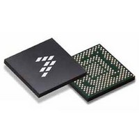
SC900841JVKR2 Freescale Semiconductor, SC900841JVKR2 Datasheet - Page 128

SC900841JVKR2
Manufacturer Part Number
SC900841JVKR2
Description
IC POWER MGT 338-MAPBGA
Manufacturer
Freescale Semiconductor
Specifications of SC900841JVKR2
Applications
PC's, PDA's
Operating Temperature
-40°C ~ 85°C
Mounting Type
Surface Mount
Package / Case
338-TBGA
Input Voltage
2.8 V to 4.4 V
Maximum Operating Temperature
+ 85 C
Minimum Operating Temperature
- 40 C
Lead Free Status / RoHS Status
Lead free / RoHS Compliant
Current - Supply
-
Voltage - Supply
-
Lead Free Status / Rohs Status
Lead free / RoHS Compliant
Available stocks
Company
Part Number
Manufacturer
Quantity
Price
Company:
Part Number:
SC900841JVKR2
Manufacturer:
Freescale Semiconductor
Quantity:
10 000
- Current page: 128 of 192
- Download datasheet (8Mb)
POWER PATH MANAGER SPI REGISTERS
POWER PATH MANAGER PLUS LI-ION CHARGER
REGISTERS AND BITS DESCRIPTION
Table 78. Charger Interrupt/Mask Registers Structure and Bits Description
128
900841
FUNCTIONAL DEVICE OPERATION
BATTERY INTERFACE AND POWER PATH MANAGEMENT
MBATOVP
Reserved
USBOVP
Reserved
BATOVP
USBDET
BATDET
DCLMT
COMP
Name
TEMP
Bits
0
1
2
3
4
5
6
7
0
1
Reserved
Battery over-voltage Interrupt Signal (V
x0 = No over-voltage condition
x1 = Over-voltage condition
Battery over/under-temperature Interrupt Signal
(Battery temperature is out of valid window)
x0 = No over/under-temperature condition
x1 = Over/under-temperature condition
Battery Charge Cycle Completion Interrupt Signal
This signal is set any time a charging cycle is complete or the RDSTATE bits change. The RDSTEN bit controls how
often this interrupt signal is asserted.
If RDSTEN is 0 the following conditions must be true for the COMP interrupt to be set:
VBAT > CHRGCV setting (V
x0 = Charge Cycle Not Complete
x1 = Charge Cycle Complete
If RDSTEN is 1 Then the following is true for the COMP interrupt
x0 = Charge Cycle Not Complete
x1 = RDSTATE register bits change
USB VBUS Detection Interrupt Signal.
This is a dual edge interrupt signal that is set any time a valid USB device (V
disconnected
x0 = No interrupts pending
x1 = USB VBUS is connected/disconnected (refer to the SCHRGINT register)
Battery Detection Interrupt Signal
This is a dual edge interrupt signal that is set any time a valid battery (VBAT > VTRKL) is connected or disconnected
x0 = No interrupts pending
x1 = battery is connected/disconnected (refer to the SCHRGINT register)
Charge Input Current Limit Detection Interrupt Signal
x0 = No Input Current Limit Detected
x1 = Input Current Limit Detected
Charge Input over-voltage Detection Interrupt Signal (V
x0 = No Input over-voltage Detected
x1 = Input over-voltage Detected
Reserved
Battery over-voltage Interrupt Signal Mask
x0 = Unmask
x1 = Mask
MCHRGINT (ADDR 0xD1 - R/W - Default Value: 0x00)
CHRGINT (ADDR 0xD0 - R - Default Value: 0x00)
CHRGCV
) & I
BAT
CHG
> V
< CHRGCOMP setting (IEOC)
CHGCV
Description
+ V
RAWCHG
OVRVOLT
> V
)
RAWCHGOVP
Analog Integrated Circuit Device Data
RAWCHG
)
> V
RAWCHGDET
Freescale Semiconductor
) is connected or
Related parts for SC900841JVKR2
Image
Part Number
Description
Manufacturer
Datasheet
Request
R
Part Number:
Description:
Ultra-mobile Platform Pmic
Manufacturer:
Freescale Semiconductor, Inc
Datasheet:

Part Number:
Description:
Sc900 Programmable Penta Uldo With Reset And I2c Interface
Manufacturer:
Semtech Corporation
Datasheet:
Part Number:
Description:
Manufacturer:
Freescale Semiconductor, Inc
Datasheet:
Part Number:
Description:
Manufacturer:
Freescale Semiconductor, Inc
Datasheet:
Part Number:
Description:
Manufacturer:
Freescale Semiconductor, Inc
Datasheet:
Part Number:
Description:
Manufacturer:
Freescale Semiconductor, Inc
Datasheet:
Part Number:
Description:
Manufacturer:
Freescale Semiconductor, Inc
Datasheet:
Part Number:
Description:
Manufacturer:
Freescale Semiconductor, Inc
Datasheet:
Part Number:
Description:
Manufacturer:
Freescale Semiconductor, Inc
Datasheet:
Part Number:
Description:
Manufacturer:
Freescale Semiconductor, Inc
Datasheet:
Part Number:
Description:
Manufacturer:
Freescale Semiconductor, Inc
Datasheet:
Part Number:
Description:
Manufacturer:
Freescale Semiconductor, Inc
Datasheet:
Part Number:
Description:
Manufacturer:
Freescale Semiconductor, Inc
Datasheet:
Part Number:
Description:
Manufacturer:
Freescale Semiconductor, Inc
Datasheet:
Part Number:
Description:
Manufacturer:
Freescale Semiconductor, Inc
Datasheet:


