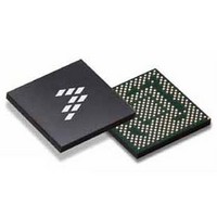
SC900841JVKR2 Freescale Semiconductor, SC900841JVKR2 Datasheet - Page 22

SC900841JVKR2
Manufacturer Part Number
SC900841JVKR2
Description
IC POWER MGT 338-MAPBGA
Manufacturer
Freescale Semiconductor
Specifications of SC900841JVKR2
Applications
PC's, PDA's
Operating Temperature
-40°C ~ 85°C
Mounting Type
Surface Mount
Package / Case
338-TBGA
Input Voltage
2.8 V to 4.4 V
Maximum Operating Temperature
+ 85 C
Minimum Operating Temperature
- 40 C
Lead Free Status / RoHS Status
Lead free / RoHS Compliant
Current - Supply
-
Voltage - Supply
-
Lead Free Status / Rohs Status
Lead free / RoHS Compliant
Available stocks
Company
Part Number
Manufacturer
Quantity
Price
Company:
Part Number:
SC900841JVKR2
Manufacturer:
Freescale Semiconductor
Quantity:
10 000
- Current page: 22 of 192
- Download datasheet (8Mb)
Table 4. Dynamic Electrical Characteristics
noted. Typical values are characterized at V
22
900841
ELECTRICAL CHARACTERISTICS
DYNAMIC ELECTRICAL CHARACTERISTICS
SPI INTERFACE TIMING AND LOGIC IO
VIDEN/VID TIMING SPECIFICATION
OSCILLATOR AND CLOCK OUTPUTS MAIN CHARACTERISTICS
RTC
VCC ELECTRICAL CHARACTERISTICS
VNN ELECTRICAL CHARACTERISTICS
Time SPICSB has to be low before the first rising edge of SPICLK
Time SPICSB has to remain low after the last falling edge of SPICLK
Time SPICSB has to remain high between two transfers
Clock period of SPICLK (Equivalent to a maximum clock frequency of 25 MHz)
Part of the clock period where SPICLK has to remain high
Part of the clock period where SPICLK has to remain low
Time MOSI has to be stable before the next falling edge of SPICLK
Time MOSI has to remain stable after the falling edge of SPICLK
Time MISO will be stable before the next falling edge of SPICLK
Time MISO will remain stable after the falling edge of SPICLK
Time MISO needs to become active after the falling edge of SPICSB
Time MISO needs to become inactive after the rising edge of SPICSB
VIDEN/VID Debounce time
VIDEN Invalid State Hold Time
RTC OSC Startup Time (Upon Application of Power)
26 MHz OSC Startup Time
RTC Clock Frequency, Crystal OSC Nominal Frequency
Transient Load Speed of Change
Soft Start Time (Enable to output voltage ramp up from 0 to 1.0 V (25 mV/s))
Turn Off Time (OFF to output voltage ramp down to 0 V)
DAC Slew Rate
Switching Frequency
Transient Load Speed of Change
Soft Start Time (Enable to output voltage ramp up from 0 V to 1.0 V (25 mV/s))
Turn Off Time (OFF to output voltage ramp down to 0 V)
DAC Slew Rate
Switching Frequency
T
A
= -40 °C to 85 °C, V
PWR
Characteristic
= 3.0 to 4.4 V, typical external component values, and full load current range, unless otherwise
DYNAMIC ELECTRICAL CHARACTERISTICS
PWR
= 3.6 V and 25 °C.
t
t
t
t
Symbol
t
t
SELHIGH
CLKHIGH
t
CLKLOW
WRTHLD
t
t
t
t
CLKPER
SELHLD
t
WRTSU
t
RDHLD
t
t
t
CCOFF
t
NNOFF
SELSU
RDDIS
RDSU
RDEN
HOLD
I
SSCC
I
SSNN
f
f
CC
NN
t
SW
SW
DB
-
-
-
-
-
/t
/t
Min
100
5.0
5.0
5.0
5.0
5.0
1.0
20
20
20
40
18
18
-
-
-
-
-
-
-
-
-
-
-
-
-
Analog Integrated Circuit Device Data
Refer to
32.768
Typ
Figure 5
1.0
1.0
25
25
-
-
-
-
-
-
-
-
-
-
-
-
-
-
-
-
-
-
-
-
-
Freescale Semiconductor
for more details
Max
0.06
0.06
400
500
1.0
1.0
1.0
1
1
-
-
-
-
-
-
-
-
-
-
-
-
-
-
-
-
-
mV/µs
mV/µs
MHz
MHz
Unit
KHz
A/ns
A/ns
ms
ms
ms
ms
ms
ms
ns
ns
ns
ns
ns
ns
ns
ns
ns
ns
ns
ns
μs
Related parts for SC900841JVKR2
Image
Part Number
Description
Manufacturer
Datasheet
Request
R
Part Number:
Description:
Ultra-mobile Platform Pmic
Manufacturer:
Freescale Semiconductor, Inc
Datasheet:

Part Number:
Description:
Sc900 Programmable Penta Uldo With Reset And I2c Interface
Manufacturer:
Semtech Corporation
Datasheet:
Part Number:
Description:
Manufacturer:
Freescale Semiconductor, Inc
Datasheet:
Part Number:
Description:
Manufacturer:
Freescale Semiconductor, Inc
Datasheet:
Part Number:
Description:
Manufacturer:
Freescale Semiconductor, Inc
Datasheet:
Part Number:
Description:
Manufacturer:
Freescale Semiconductor, Inc
Datasheet:
Part Number:
Description:
Manufacturer:
Freescale Semiconductor, Inc
Datasheet:
Part Number:
Description:
Manufacturer:
Freescale Semiconductor, Inc
Datasheet:
Part Number:
Description:
Manufacturer:
Freescale Semiconductor, Inc
Datasheet:
Part Number:
Description:
Manufacturer:
Freescale Semiconductor, Inc
Datasheet:
Part Number:
Description:
Manufacturer:
Freescale Semiconductor, Inc
Datasheet:
Part Number:
Description:
Manufacturer:
Freescale Semiconductor, Inc
Datasheet:
Part Number:
Description:
Manufacturer:
Freescale Semiconductor, Inc
Datasheet:
Part Number:
Description:
Manufacturer:
Freescale Semiconductor, Inc
Datasheet:
Part Number:
Description:
Manufacturer:
Freescale Semiconductor, Inc
Datasheet:


