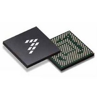
SC900841JVKR2 Freescale Semiconductor, SC900841JVKR2 Datasheet - Page 71

SC900841JVKR2
Manufacturer Part Number
SC900841JVKR2
Description
IC POWER MGT 338-MAPBGA
Manufacturer
Freescale Semiconductor
Specifications of SC900841JVKR2
Applications
PC's, PDA's
Operating Temperature
-40°C ~ 85°C
Mounting Type
Surface Mount
Package / Case
338-TBGA
Input Voltage
2.8 V to 4.4 V
Maximum Operating Temperature
+ 85 C
Minimum Operating Temperature
- 40 C
Lead Free Status / RoHS Status
Lead free / RoHS Compliant
Current - Supply
-
Voltage - Supply
-
Lead Free Status / Rohs Status
Lead free / RoHS Compliant
Available stocks
Company
Part Number
Manufacturer
Quantity
Price
Company:
Part Number:
SC900841JVKR2
Manufacturer:
Freescale Semiconductor
Quantity:
10 000
- Current page: 71 of 192
- Download datasheet (8Mb)
VNN
synchronous Buck PWM voltage mode control DC/DC
regulator, designed to power high performance CPUs. VNN
uses external MOSFETs, P-ch high side and N-ch low side.
requirements. A 7-bit DAC reads the VID input signals and
sets the output voltage level. The output voltage has a range
of 0.3 to 1.2 V. The programming step size is 12.5 mV.
Values will be read in real time and will be stored in internal
registers not accessible to the system host. Reference
VIDEN[1:0] & VID[6:0]
VNN, where a latch signal for each regulator decides which
regulator takes control of the VID input signals.
output voltage node is connected directly to the inverting
input of the error amplifier that uses the DAC output as its
reference, unity gain configuration. Using this configuration
Main Features
• Uses the V
• It is used to provide power to the Graphics Core.
• Single-Phase Solution with Integrated Drivers and
• VID Controlled for dynamic voltage scaling requirements
• 1.0 MHz switching frequency
• High efficiency operating modes depending on load
Analog Integrated Circuit Device Data
Freescale Semiconductor
This is a VID controlled single-phase 1.0 MHz 2-switch
VNN includes support for VID active voltage positioning
The same VID input signals are shared between VNN and
The DAC value represents the output voltage value. The
external MOSFETs
of high performance processors
conditions
PWR
C
V
rail as its power supply
ONN
NN
Pins.
C
L
NN
INCC
V
PWR
Figure 25. VNN Detailed Internal Block Diagram
M
M
HSNN
LSNN
VOUTFBNN
SWFBNN
HSNNGT
PGNDNN
PVINNN
LSNNGT
CSPNN
Current Sense
Internal
Compensation
Driver
Z1
Amp
I
NN
with internal compensation eliminates the need for the
feedback and compensation network, which saves board
space and cost. The DAC/output voltage slew rate is
internally set 25 mV/µs to minimize transient currents and
audible noise.
the load conditions. These modes can be set through the SPI
and include a PFM mode, an Automatic Pulse Skipping
mode, and a PWM mode. The previous selection is optimized
to maximum battery life based on load conditions.
down.
on VCC regulator. (See VCC)
current protection. If an over-current condition is detected,
the regulator will limit the current through cycle by cycle
operation and alert the system through the VNNFAULT
signal, which will in turn assert the VRFAULT Interrupt signal.
• Output can be discharged through the low side switch.
• Loss-Less Output Current Sensing with over-current
• Uses internal compensation
• Gate drive circuits are supplied directly from VPWR
Efficiency Curves
mode based on the recommended external component
values and typical output voltage of 1.2. 3.0 V ≤ VPWR ≤
4.4 V.
EA
Z2
The switcher can operate in different modes depending on
VNN will be discharged every time the regulator is shutting
The output current is sense in the same way as it is done
The sensed output current value will also be used for over-
protection
The following efficiency curves are calculated under PWM
Controller
DAC
AOACCTLVNN
VNNFAULT
CTLVNN
FUNCTIONAL DEVICE OPERATION
VIDEN0
VIDEN1
V
REF
Interface
SPI
POWER SUPPLIES
900841
71
Related parts for SC900841JVKR2
Image
Part Number
Description
Manufacturer
Datasheet
Request
R
Part Number:
Description:
Ultra-mobile Platform Pmic
Manufacturer:
Freescale Semiconductor, Inc
Datasheet:

Part Number:
Description:
Sc900 Programmable Penta Uldo With Reset And I2c Interface
Manufacturer:
Semtech Corporation
Datasheet:
Part Number:
Description:
Manufacturer:
Freescale Semiconductor, Inc
Datasheet:
Part Number:
Description:
Manufacturer:
Freescale Semiconductor, Inc
Datasheet:
Part Number:
Description:
Manufacturer:
Freescale Semiconductor, Inc
Datasheet:
Part Number:
Description:
Manufacturer:
Freescale Semiconductor, Inc
Datasheet:
Part Number:
Description:
Manufacturer:
Freescale Semiconductor, Inc
Datasheet:
Part Number:
Description:
Manufacturer:
Freescale Semiconductor, Inc
Datasheet:
Part Number:
Description:
Manufacturer:
Freescale Semiconductor, Inc
Datasheet:
Part Number:
Description:
Manufacturer:
Freescale Semiconductor, Inc
Datasheet:
Part Number:
Description:
Manufacturer:
Freescale Semiconductor, Inc
Datasheet:
Part Number:
Description:
Manufacturer:
Freescale Semiconductor, Inc
Datasheet:
Part Number:
Description:
Manufacturer:
Freescale Semiconductor, Inc
Datasheet:
Part Number:
Description:
Manufacturer:
Freescale Semiconductor, Inc
Datasheet:
Part Number:
Description:
Manufacturer:
Freescale Semiconductor, Inc
Datasheet:


